The rise of 800V high voltage DC: can collaboration drive NVIDIA’s AI infrastructure vision?

NVIDIA’s transition to an 800 VDC architecture for AI data centres is a technological shift that will demand industry-wide alignment on power delivery, semiconductors and standards.
By Rebecca Pool, Technology Editor.
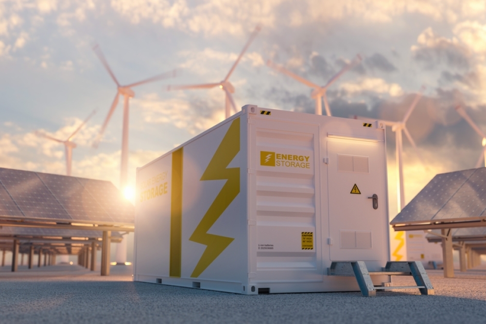
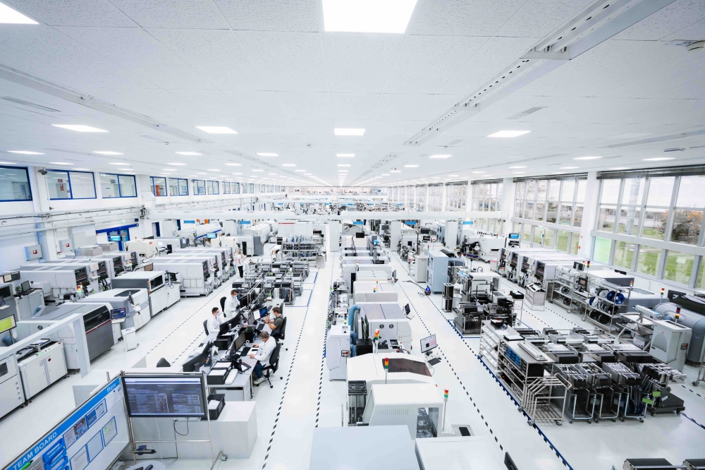
When NVIDIA first announced its 800 V high-voltage direct current architecture for AI servers and data centres in May this year, it wasn’t a huge surprise. AI servers, especially those using GPUs and accelerators, were already drawing up to ten times more power per rack than traditional servers, and your 48 and 54 VDC distribution systems were suffering major power losses.
The shift to the higher voltage bus aims to address these issues, raising power efficiency and density in the data centre infrastructure of tomorrow.
As NVIDIA senior power architect, Jared Huntington, and colleagues, said in their blog at the time : “Traditional 54 V in-rack power distribution, designed for kilowatt-scale racks, isn’t designed to support the megawatt-scale racks coming soon to modern AI factories.
[We are] leading the transition to 800 VDC data centre power infrastructure to support 1 MW IT racks and beyond, starting in 2027.”
Power distribution in today’s data centres involves multiple voltage conversions, introducing inefficiencies into the electrical system. But by moving to this new architecture - in which AC grid power can be directly converted to 800 VDC at the data centre - many conversion steps will be eliminated, reducing energy losses during AC/DC and DC/DC transformations. Clearly the 800 VDC shift hinges on industry-wide coordination on voltage ranges, connector interfaces and supporting standards – but from word go, numerous partners pledged support.
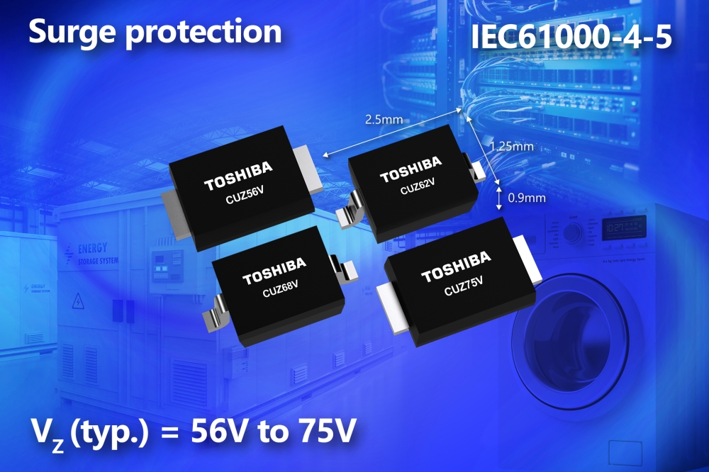
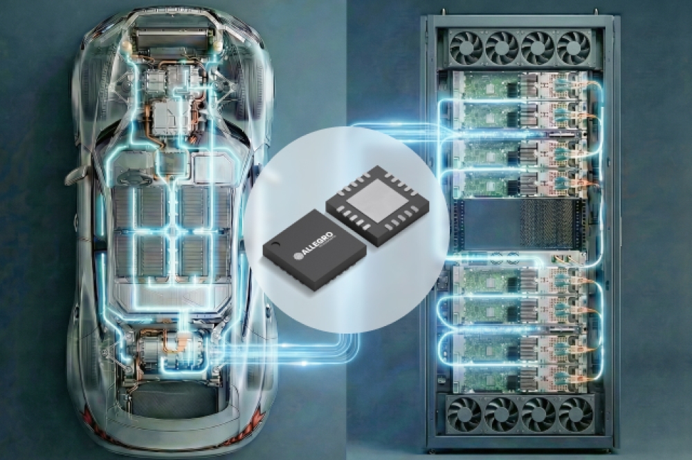
Early on, Infineon highlighted how it will apply its expertise in silicon, SiC and GaN semiconductors in a collaboration with NVIDIA to ‘create new power delivery standards’ for AI data centres. The Germany semiconductor heavyweight pointed out how the future system architecture will be centralized, making the best possible use of the constraint space in a server rack – increasing the importance of power semiconductor solutions using fewer power conversion stages and allowing upgrades to even higher distribution voltages.
Onsemi, which has long-developed both silicon and SiC semiconductors, and GaN device manufacturer, Innoscience, both trumpeted support for NVIDIA’s transition to 800 VDC power architectures. And Navitas was also quick to announce that its GaN and SiC power semiconductors will support NVIDIA’s Kyber rack-scale systems powering AI-accelerating GPUs, such as ‘Rubin Ultra’. The US firm highlighted that NVIDIA’s 800 VDC architecture is expected to improve end-to-end power efficiency by up to 5%, reduce maintenance costs by 70% and lower cooling costs by directly connecting the HVDC to the IT and compute racks.
Other semiconductor providers offering support include Analog Devices, AOS, EPC, MPS, Renesas, Richtek, ROHM, STMicroelectronics and Texas Instruments. Meanwhile additional support has come from power system components partners, such as BizLink, Delta, Flex Power, GE Vernova, Lead Wealth, LiteOn and Megmeet, as well as data centre power system providers, including ABB, Eaton, Mistubishi Electric and Schneider Electric.
Setting standards
Since the initial reaction to NVIDIA’s plan to lead industry towards to the 800 VDC architecture, even more announcements relating to next-generation data centres have followed – particularly at the Open Compute Project (OCP) Global Summit, in October. For starters, the OCP - recognised as a crucial forum for establishing open standards for hardware designs and specifications - unveiled its ‘Open Data Center for AI’ strategic initiative, with initial support from Google, Meta and Microsoft. The initiative expands on the OCP’s Open Systems for AI initiative, and aims to develop the necessary standards so the already rapidly-evolving AI data centre infrastructure can be flexibly deployed alongside traditional systems.
According to OCP Chief Innovation Officer, Dr Clifford Grossner, the initiative was a “natural evolution” of work the organisation had started some 18 months ago, knowing that a transition from cloud data centres to AI data centres was coming. “If you look at a typical enterprise, one rack of equipment might consume 20 to 30 kW of power... when we start to move towards architectures with GPUs and building AI clusters, we are already approaching several hundred kilowatts and we can envision at least one megawatt racks in the future,” he explains.
“We also realised that AI workloads aren’t like cloud workloads... and [involve] massively parallel computation so the power draw may go from very small to very large, very quickly,” he adds. “[Factor in] that the AI data centres of the future might draw as much power as a small city, and we knew the time was right to understand the ways that we can bring standardizations here and solve problems in a collaborative fashion.”
Tech giants have already contributed several OCP specifications. For example “Diablo” from Google, Meta and Microsoft describes a high-density sidecar rack for powering AI clusters. Meanwhile AMD, Google and Microsoft have co-authored “Hyperscale CPU Reliability, Availability, and Serviceability (RAS) and debug requirements for CPUs”.

NVLink Fusion enables partners, such as Fujitsu and Qualcomm, to couple custom CPUs with NVIDIA GPUs in a rack-scale architecture to boost AI performance. [NVIDIA]
Such specifications can only help to accelerate the deployment of AI data centres, but as Grossner emphasises: “We don’t stop at specifications – we want products, and so we’re going to be building the multi-vendor supply chain that can supply this equipment.”
Many in industry agree the time is ripe for unified industry action on future AI data centre requirements. “With the AI infrastructure market moving very fast, there is a risk of higher costs due to fragmentations,” commented Technology Analyst, Alan Weckel of 650 Group. “It is the right time for an organization like the OCP to be facilitating a community to determine commonalities in data centre facilities and IT infrastructure that can help accelerate the market for future generations of AI cluster deployments and data centre facility builds.”
Weckel’s comments echoed across numerous plenary presentations from tech executives at the OCP Global Summit. Microsoft’s Saurabh Dighe, Corporate VP, Azure Strategic Planning and Architecture, highlighted how colleagues have re-engineered the entire stack from system to silicon to deploy AI, with the design being contributed to OCP. ARM Senior Vice President of Infrastructure, Mohamed Awad, also described how the company has been working with OCP on chiplet system architecture specifications. “It’s unclear to me if we’ll ever get to a truly interoperable chiplet marketplace, but there’s no reason we can’t work together to define a common system architecture,” he said. “This would meaningfully accelerate time to market and innovation... and allow for new dimensions of systems optimization that are too complex for most companies to take on by themselves.”

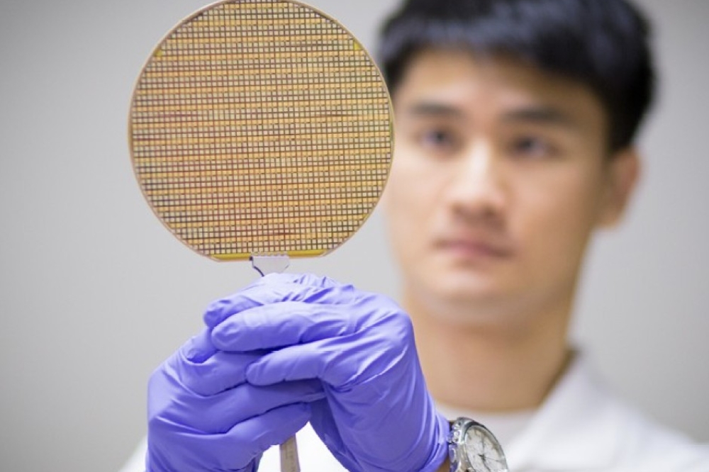
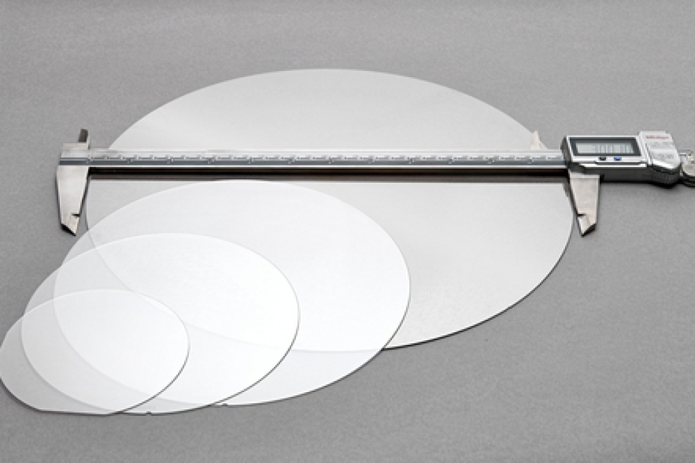
Microchip president and chief executive, Steve Sanghi, with a 3nm wafer: the firm’s Gen 6 PCIe switches are manufactured using a 3 nm process. [Microchip]
Collaborating on complexity
Plenaries aside, the flurry of products and white papers describing power architecture components and plans from semiconductor players at the OCP Summit signify a meeting of minds on the complexity that is to come, and the will to tackle issues head on. Infineon, EPC, Alpha and Omega Semiconductor, and a host of other industry players announced developments to support the power demands of NVIDIA’s 800 VDC architecture.
Texas Instruments debuted a dual-phase smart power stage, a reference design for a 30 kW AI server power supply unit and a GaN intermediate bus converter that can convert energy down from 800 VDC to a lower intermediate bus voltage – all to address the growing power consumption in next-generation data centres. “The transition to an 800 VDC power architecture fosters a renewed discussion about how to design power delivery [within an IT server rack] given the trade-offs in overall conversion efficiency, size and performance,” TI stated in its white paper, ‘Power delivery trade-offs when preparing for the next wave of AI computing growth’.
In a similar vein, Renesas outlined how GaN semiconductors can benefit the data centres of tomorrow, describing how power devices can be used in new architectures as well as sidecar AC/DC racks, for efficient, high-frequency power conversion at the higher voltages and power densities. The Japan-based semiconductor supplier also highlighted how its silicon REXFETs can support future designs. “[We are] helping power the future of AI with high-density energy solutions built for scale, supported by our GaN FETs, MOSFETs, controllers and drivers,” said Zaher Baidas, Senior Vice President and General Manager of Power at Renesas. “[Such] innovations will deliver performance and efficiency, with the scalability required for future growth.”
Power Integrations also outlined how high voltage GaN HEMTs can deliver high power density and efficiency in 800 VDC power architectures. And in another example, Microchip revealed what it calls the industry’s first 3 nm PCIe Gen 6 switch, designed to reduce power consumption in high density AI systems when connecting and routing high speed data between critical compute resources such as CPUs, GPUs, AI accelerators and storage devices. Systems level player Flex Power also launched an open platform integrating power, cooling and compute resources into modular designs for next-generation data centres while Eaton unveiled a reference architecture for 800 VDC power systems.
More than hardware
In May this year, NVIDIA also introduced ‘NVLink Fusion’, a system for partners to integrate their own silicon AI processors with the firm’s GPU ecosystem using NVLink, interconnect technologies designed to connect NVIDIA GPUs and CPUs. Custom silicon and technology partners include MediaTek, Marvell, Alchip, Astera Labs, Global Unichip Coporation, Samsung, Synopsys and Cadence while CPU partners are Fujitsu, Qualcomm Technologies and Intel.
Prior to NVLink Fusion, NVLink technologies could only be used with NVIDIA chips - and while Fusion drives demand for NVIDIA’s underlying AI infrastructure amongst hardware developers, it also lowers the barrier to developing and scaling data centre infrastructure. In his recent technical blog, ‘Scaling AI Inference Performance and Flexibility with NVIDIA NVLink and NVLink Fusion’, Joe DeLaere, NVIDIA senior manager for accelerated computing solutions for data centre, wrote: “Being available as a modular Open Compute Project (OCP) MGX rack solution enables NVLink Fusion integration with any network interface card, data processing unit or scale-out switch, giving customers the flexibility to build what they need.”
Importantly, NVIDIA’s NVLink Fusion, twinned with recent strategic partnerships, also indicate the firm is positioning itself not just as a straightforward AI infrastructure provider, but moreover, as a collaborative platform for future AI-driven computing. As industry barrels towards the modern AI data centre, this openness will be critical to power semiconductor firms developing the devices that will support AI data centre scaling and the ensuing rises in energy consumption.
And of course, for OCP, openness remains fundamental. In October, this year, the organisation welcomed three data centre powerhouses to its Board of Directors, reflecting the importance of collaboration amongst hyperscalers, semiconductor firms and infrastructure providers.
“We’ve expanded our board with AMD, ARM and NVIDIA,” explains Grossner. “And just as ARM is bringing its chiplet ecosystem to OCP, we’re encouraging NVIDIA to do the same around NVLink.”
“The impact of [AI data centres] is becoming really obvious and real,” he adds. “We’d be remiss to not take action and avoid serious issues.”