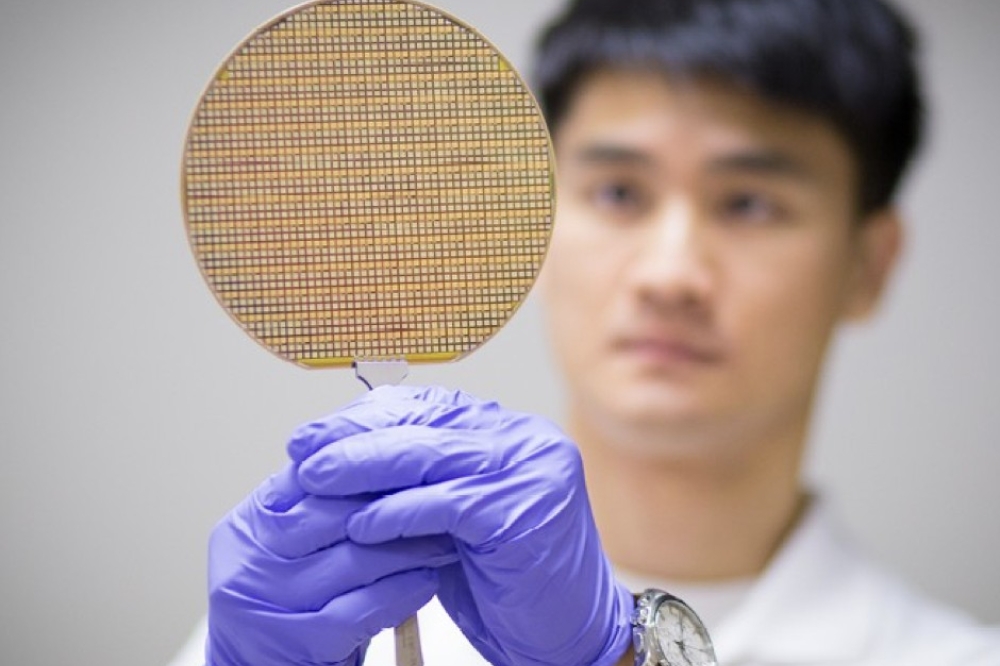
USTC team develops GaN/diamond CMOS power circuit
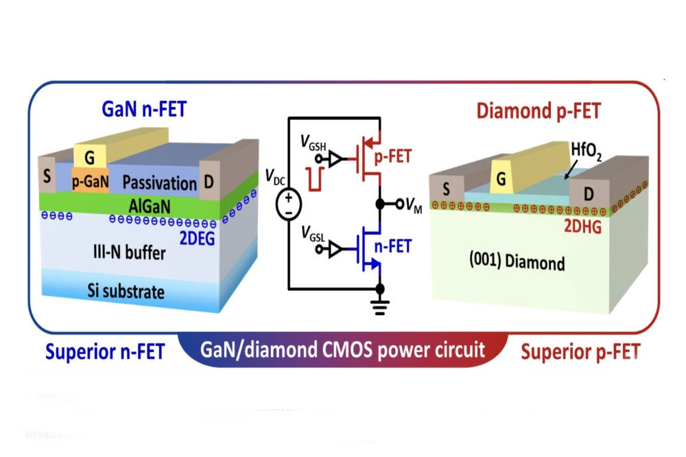
Researchers from the University of Science and Technology of China (USTC) and collaborators have manufactured a high-performance normally-off diamond p-FET featuring high-density 2D hole gas (HG) with high hole mobility, tackling the fundamental challenge towards highly conductive wide-bandgap p-FETs.
According to the team, this achievement enables the world’s first GaN/diamond complementary (CMOS) power circuit with highly matched p/n-channel conduction capability and superior switching performance at high voltage and high frequency.
CMOS configuration, comprising an upper p-FET and a lower n-FET, plays a dominant role in today’s microelectronics industry. In power electronics, compared with the conventional topology with n-FETs connected in series, CMOS power configuration can also overcome the crosstalk issue during high-frequency and high-voltage switching transients.
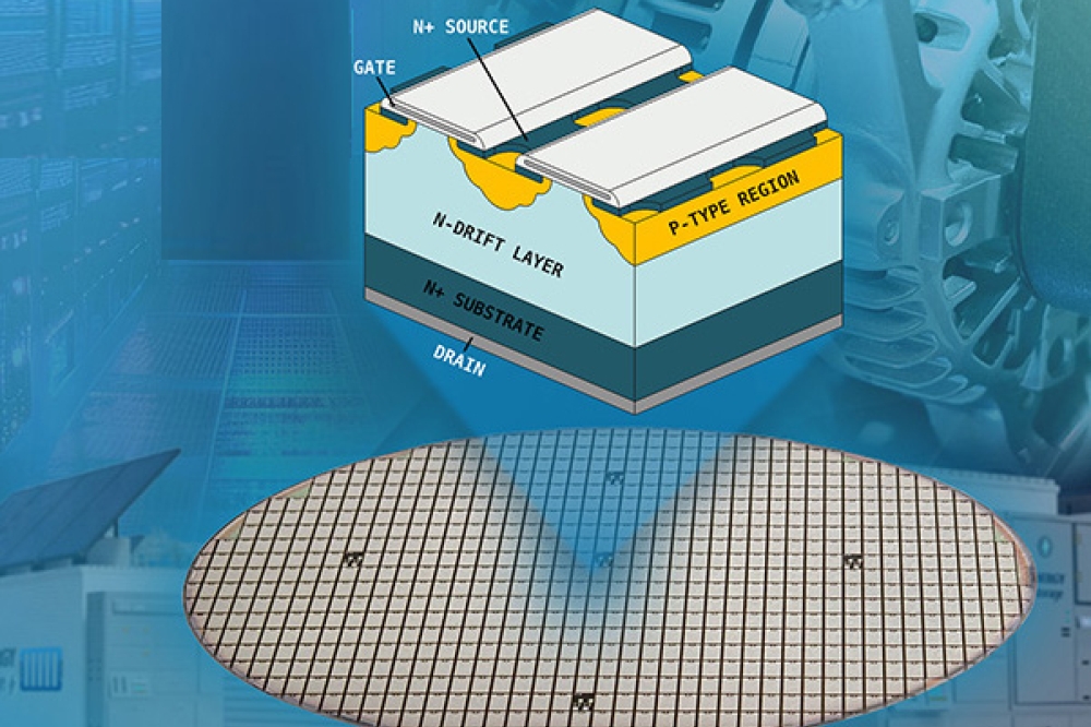
Wide-bandgap (WBG) semiconductors enable high-power-density and high-efficiency power conversion. GaN HEMT with two-dimensional electron gas (2DEG) and high electron mobility is an excellent choice for n-FET. However, most WBG semiconductors (GaN, Ga2O3, etc.) suffer from low hole mobility (10~15 cm2/V·s for GaN) or even difficulty in p-type doping, such that it has been fundamentally challenging to realise high-performance p-FET and well-matched p/n power FETs.
Alternatively, hydrogen-terminated diamond can form a high-density two-dimensional hole gas (2DHG) with hole mobility of 10~20 times higher than that in GaN. The WBG diamond p-FET and GaN n-FET featuring 2DHG/2DEG and well-matched conduction performance are compelling choices for building a CMOS power circuit.
The USTC team has developed a high-performance diamond p-FET with desirable normally-off operation by employing low-work-function Ti gate metal to deplete the 2DHG in the gate region. In the meantime, a highly conductive 2DHG is maintained in the gate-to-drain access region, delivering a high on-state current of ~1900 A/cm2. This p-FET yields a high power figure-of-merit of 10.34 MW/cm², which is the best among the state-of-the-art normally-off diamond and GaN p-FETs.
Thanks to the highly conductive 2DHG in diamond, the diamond p-FET and GaN n-FET exhibit well-matched conduction performance with similarly low on-resistance (3~5 mΩ·cm2), whereas the on-resistance of GaN p-FET is generally 100 times higher than that of GaN n-FET. Furthermore, the highly symmetric gate driving voltages of p-FET (-5 V) and n-FET(+5 V) promise to simplify the gate driving scheme.
The USTC team has successfully demonstrated the world’s first CMOS power circuit based on high-mobility p/n-channel diamond/GaN transistors. Unlike the n-FET-only power circuit suffering from high-frequency crosstalk and false turn-on due to the floating source potential of the upper n-FET, this CMOS power circuit with fixed source potential of the upper p-FET successfully obliterates the high-frequency crosstalk and enhances the circuit reliability during high-voltage and high-frequency switching.
Future plans include electric field engineering to further increase the power figure-of-merit of diamond p-FET, and fabrication of large-area multi-finger devices to boost the power handling capability.
Pictured above: Schematic of CMOS power circuit configuration featuring well-matched upper diamond p-FET and lower GaN n-FET with 2DHG/2DEG.
Reference
Chenyue Chu, Shu Yang et al., 71st IEEE International Electron Devices Meeting (IEDM), p. 26.8.1, 2025.