Metrology for the 2 nm era and beyond
Infinitesima bets on high-speed atomic force microscopy to keep advanced silicon on track.
BY REBEECCA POOL, TECHNOLOGY EDITOR
WITH Taiwan’s lead chipmaker, TSMC, set to begin full-scale production of 2 nm technology, silicon chip design is entering uncharted territory – and pulling metrology along with it.
As ever-more complex 3D architectures, complementary-FETs, hybrid bonding and advanced packaging emerge, metrology and inspection tools will be vital to robust chip fabrication. But with transistor dimensions shrinking to just a few atoms, the workhorse of defect detection - optical inspection – is hitting its limits.
Deep UV lithography at 193 nm wavelength has already given way to extreme UV (EUV) lithography at 13.5 nm. Yet the smallest etch patterns now measure as small as 9 nm.
Factor in intricate buried structures with remarkably high aspect ratios and more than 100 stacked layers on a single chip, and the challenge of detecting defects becomes staggering.
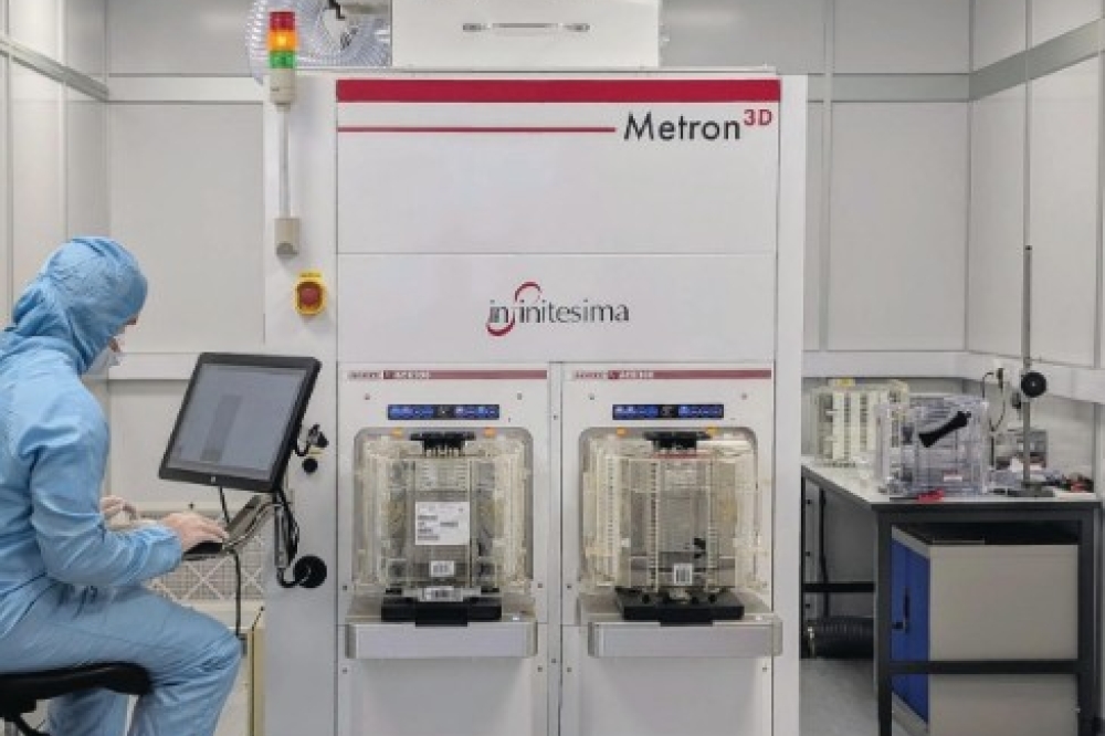
One company that remains undeterred is UK-based Infinitesima, which has just joined forces with photolithography systems giant, ASML, of The Netherlands, and Belgian R&D powerhouse, IMEC, to hone its in-line metrology platform for increasingly complex device architectures.
Instead of the usual optical methods, ‘Metron3D’ relies on atomic force microscopy (AFM), where a probe tip oscillates above the silicon wafer surface and measures the atomic forces, to detect defects. The platform combines AFM with interferometry and other optics innovations to increase inspection throughput of structures by at least 100 times compared to standard AFM - critical for defect detection on a high volume semiconductor manufacturing line.
Together the partners now intend to optimise and drive Infinitesima’s unconventional metrology tech further into the silicon semiconductor market. “Industry is operating at the atomic-scale to control transistors – for example, to store electrons in a capacitor, very complex 3D structures are being [fabricated] and that’s creating a need for sub-nanometre 3D metrology,” says Infinitesima CEO, Peter Jenkins. “AFM is good at this, but traditionally very slow. So solving the speed problem means customers have the metrology to move these structures from R&D and into volume manufacturing.”
From lab roots to fab floors
Founded in 2001 by University of Bristol professor, Andrew Humphris, to commercialise fast scanning probe microscopy for biological samples, Infinitesima quickly switched to semiconductors – given the greater market potential. The company’s rapid probe microscope (RPM) soon followed - essentially a high-speed AFM that uses optical interferometry, instead of laser beam deflection, to track the AFM probe tip’s motion and enable faster sample scanning.
Come 2010, photothermal actuation had replaced mechanically or piezoelectrically-driven actuation in the RPM set-up, to reliably drive probe tips at higher frequencies.
This helped to cut surface analysis and defect detection from minutes to seconds while still delivering sub-nanometre vertical resolution – proving the technique viable for semiconductor fabs. RPM technology was later integrated to Carl Zeiss’ photomask repair tools as well as the scanning electron microscope platforms of a leading US chipmaker.
“It’s the optics that give RPM its speed and enable unique modes of operation, helpful for looking at small, high aspect ratio structures on semiconductors,” highlights Jenkins. “We currently dither [oscillate] the probe at 600 kHz and will extend this to more than a megahertz in the future to enable even faster speeds”.
Scaling to volume production
With RPM in tow, Infinitesima partnered with IMEC to integrate its technology with wafer-handling software, robotics, and a high-speed wafer stage, to provide in-line metrology for next- generation logic, DRAM and 3D NAND. Metron3D was delivered in late 2021, and backed by Asia-based investors as well as Applied Ventures, the venture arm of US semiconductor equipment heavyweight, Applied Materials, Infinitesima has been ramping production ever since.
Right now, R&D and core module manufacturing takes place in the UK, with system assembly in Taiwan. “We don’t have to invest in building a factory and it’s going to be much faster to scale [manufacturing],” says Jenkins.
The system has already shipped to a significant - but unnamed - Taiwan- based foundry as well as to high bandwidth memory chip maker, SK Hynix of Korea - also a supplier to AI giant Nvidia - for advanced DRAM inspection. As Young-Hyun Choi, Head of Defect Analysis, Metrology and Inspection Technology, has said: “3D process control at the nano-scale level is becoming increasingly important to ensure high yield in advanced DRAM processes. Metron3D has demonstrated excellent sub-nanometre 3D metrology with the required cost-of- ownership necessary for high volume manufacturing implementation.”
Next steps
Building on this traction, Infinitesima is now working with IMEC and ASML to hone Metron3D for in-line metrology of complex devices, in volume production. ASML in particular has a vested interest in optimising the platform for high- numerical aperture EUV lithography, having shipped these first resist imaging systems in early 2024.
Meanwhile, Jenkins sees other key market opportunities in 3D logic device structures such as complementary field- effect transistors (CFETs), and in hybrid wafer bonding.
“Nearly every future device will use hybrid wafer bonding, and measuring these extremely very flat [structures] is an ideal application for AFM,” he says. “AFM is one of the ground-truth metrology methods that can give you sub-nanometre, 3D information, which is why we’re confident industry will need this technology as it moves forward – and we can do this so much faster with Metron3D.”
As part of a three-year development project, the partners will focus on taking in-depth 3D surface detection, high- speed imaging and interferometric accuracy further.
By way of example, Jenkins notes they will refine the RPM probe tip and AFM operating modes to measure the smaller patterns and strut features formed on wafers during high-NA EUV lithography. “We won’t be redesigning our system,” he explains. “This is about enhancing operation within the software, codes and types of probes that we use, and the data analysis that we run. Jenkins is hopeful that come the project-end, AFM technology market growth will be well and truly on the rise. He estimates the value of today’s
AFM market at around $200 million but based on a steady semiconductor industry CAGR of 8%, expects this figure could reach $1 billion come 2030. “AFM will become increasingly complementary to certain process control steps, and the number of those steps will increase as fabrication processes evolve,” he says.
But will industry demand for Metron3D also rise? Jenkins thinks so, highlighting Infinitesima’s two existing contracts, and also noting how the technology is under evaluation with industry’s other key players – that includes Intel, Samsung and Micron.
“We’re pretty hopeful that we will see additional contracts with other players in the coming 12 to 24 months,” he says. “Time to market is critical and we already have some strong IP protecting our core technology,” he adds. “I would imagine we’ll get an [acquisition] offer from one of the lead firms down the road, which we’ll evaluate at that point in time. But for now, we’re happy doing our thing.”