iDEAL charts a new course for silicon

Will the latest MOSFET from iDEAL Semiconductor redefine silicon chip performance?
BY REBECCA POOL, TECHNOLOGY EDITOR
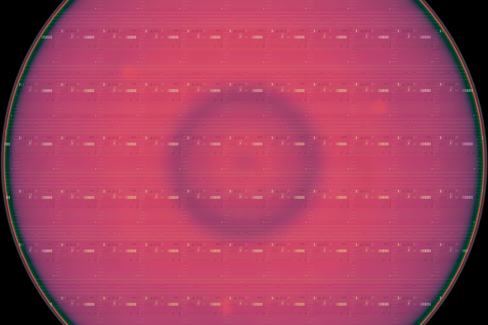
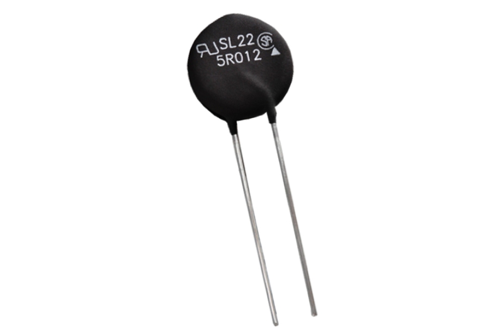
In September this year, a new kind of silicon MOSFET entered mass production. Developed by iDEAL Semiconductor, the 150V and 200V devices are based on the so-called SuperQ architecture, which the US- based firm claims is the first major advance in silicon MOSFET technology in more than 25 years.
Drawing on elements of the legacy HEXFET and Superjunction topologies, the SuperQ-based MOSFET concept was first conceived more than a decade ago. While built mostly on established CMOS processes, the device is said to break through long- standing silicon barriers in switching and conduction.
“The number one question I get from applications and systems engineers is what’s the catch?” says Ryan Manack, Vice President of Marketing at iDEAL Semiconductor. “I see competitors making devices with a lower resistance and double the switching loss, but we’re providing the next level of performance without a trade-off.”

The 150V and 200V MOSFETs are just the beginning. iDEAL Semiconductor intends to soon provide a 650 V device, and has bold plans to take its SuperQ architecture up to 1200 V.
“We’ve already demonstrated that the performance of our [structures] is either equal or better than the industry- leading super-junction structures that industry has been optimising for the last twenty years,” highlights Manack’s colleague, Philip Rutter, Vice President of Development at iDEAL Semiconductor. “We’re just getting started.”
A different approach
The SuperQ architecture follows a long history of MOSFET innovation. The legacy HEXFET architecture was launched by International Rectifier back in late 1978. Its hexagonal cell geometry in a vertical MOSFET design boosted transistor density, shrank die size, and proved pivotal to the miniaturization of electronic devices. A wide n-type conduction region helped the device to excel at low and medium voltages, but performance became inefficient at higher levels, as blocking more voltage in this drift region drove up on- resistance.
Come 1998, Infineon Technologies (then Siemens Semiconductor) changed the game with its superjunction MOSFETs, which were based on the Reduced Surface Field - RESURF - structure and could operate at higher voltages more efficiently. The drift region of this power transistor comprised pillars of p-type and n-type layers, in contrast to purely n-type material in the HEXFET, yielding a less resistive structure that could still block higher voltages.
But while this superjunction approach became the gold standard for silicon MOSFETs, higher voltage operation has demanded thick, high resistance drift regions, that can stifle silicon performance and generate excess heat. Given this, Mark Granahan, now CEO of iDEAL Semiconductor, had the idea to bring back HEXFET’s wide n-type conduction region but introduce dielectric-filled deep trenches. This novel design minimized the need for p-type layers and reduced on- resistance whilst maintaining the all-important high voltage blocking capabilities.
iDEAL Semiconductor launched in 2017, with Granahan and colleagues spending some time finding the best way to etch high aspect ratio trenches and create functional structures. They settled on atomic layer deposition, a gas-phase chemical process in which thins films are deposited one atomic layer at a time. Following several investment rounds that brought in more than $75 million, including funds from Applied Ventures, the venture capital arm of Applied Materials, so-called SuperQ technology was introduced in 2023.
“We have extremely good process control that costs less [than superjunction fabrication],” highlights Rutter. “We etch our trench and then deposit a charged layer, using atomic layer deposition.”
“So as our competitors have kept on shrinking the n-type region, they’ve lost part of the benefits [of silicon] but SuperQ trench technology promises near-ideal charge balance, allowing thinner epitaxy. It also allows a higher doping concentration in the conduction region, helping to reduce channel resistance and lowering power loss. [iDEAL Semiconductor] with SuperQ, we’ve kept the n-type region wider and have in effect just shrunk the p-region,” he adds. “From an architectural point of view, there are no limits to doing this.”

Delivering devices
Working with US-based independent foundry, Polar Semiconductor, iDEAL Semiconductor’s first devices, both 150 V and 200 V MOSFETs entered full production within weeks of each other, this Summer, and higher voltage devices are set to follow soon.
“We’ve got 300 V and 400 V MOSFETs entering the fab right now, and 650 V [devices] are in the works,” says Manack. “And [to deliver these], we’re talking quarters not years.”
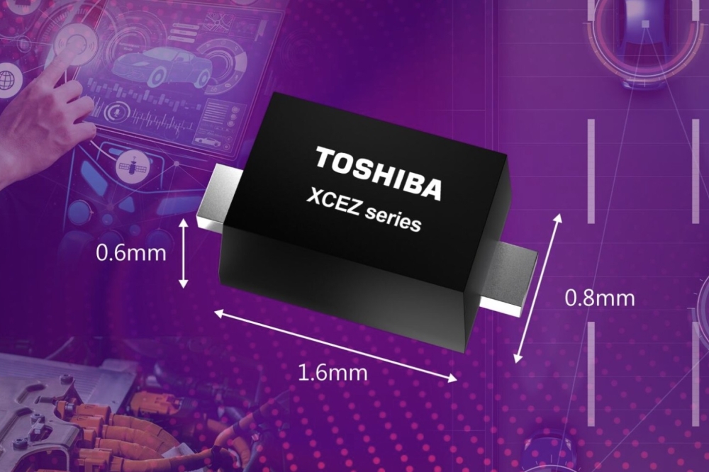
Both devices are said to reduce switching losses by at least 2X compared to competing devices, and improve resistance and power losses – whilst maintaining the benefits of silicon, including its high-volume manufacturability. The company’s latest lowest-resistance 200 V devices achieve a maximum RDS(on) of just 5.5 mΩ, delivering resistance that is said to be 1.2x lower than the current market leader, and 1.7x lower than its next-best competitor in silicon. Target applications include motor drives and AI servers, as well as LED lighting, battery protection, isolated DC/DC power modules and USB-PD adapters.
But there’s more to SuperQ than silicon MOSFETs. The technology is also designed for IGBTs, diodes, power ICs - and even other semiconductor materials, including SiC and GaN. Manack also notes that iDEAL Semiconductor’s silicon roadmap takes the technology to 1200 V.
“To reach higher voltages with the superjunction MOSFET, you grow additional epi-layers to get that thicker drift [region], which just gets more and more expensive as you get charged based on the numbers of process steps in the fab,” he says. “But we’re different. If you want a higher voltage, you need a deeper trench, so we look at how deep can we dig that trench - what aspect ratio can we reach? We believe that one day SuperQ will deliver a 1200 V MOSFET.”
Etching ever-deeper, high-aspect-ratio trenches for higher-voltage MOSFETs is no small feat, but it’s one that Rutter and colleagues believe they have mastered. With a newly acquired state-of-the-art trench etcher driving progress, they are now focused on integrating these deeper trenches into the MOSFET design - with qualification to follow. But how has the market responded to a new, high voltage MOSFET platform that is not based on wide bandgap semiconductors? High performance, energy efficient SiC and GaN devices from the likes of Wolfspeed, Infineon, EPC, Transphorm and more, have already made many in-roads into traction inverters, power supplies, fast chargers and myriad other applications. And despite recent upheavals, such as Wolfspeed’s bankruptcy and TSMC pausing GaN production, market forecasts remain robust. Still, high performance and forecasts aside, these materials remain relatively expensive and can face supply bottlenecks compared with standard silicon used in most chips. Both Manack and Rutter are keen to emphasise how SuperQ MOSFETs can be cost-effectively manufactured with tools and processes commonly standard to CMOS fabs. Rutter points out that around 90% of SuperQ’s production relies on established techniques used to fabricate vertical power trench devices while Manack notes that initial development took place on 300 mm CMOS.
“Having SuperQ on a silicon platform leverages a tremendous amount of existing tool-sets, and makes it very scalable,” adds Manack. “We’re not just increasing performance, we’re also keeping costs under control.” Recent partnerships with semiconductor distribution firms indicate that industry players agree. In July this year, iDEAL Semiconductor signed a global distribution agreement with Mouser Electronics, and also partnered with Richardson Electronics to gain access to its design and sales teams to expand the reach of its SuperQ MOSFETs.
“Some of the rhetoric in the industry has been that silicon is dead and you need to change materials and invent new tool-sets to improve performance,” reflects Manack. “But this couldn’t be further from the truth – what was dead was the new ideas and the R&D dollars.” with SuperQ, we’ve kept the n-type region wider and have in effect just shrunk the p-region,” he adds. “From an architectural point of view, there are no limits to doing this.”