Powering the AI era: how Infineon Technologies’ SiC solutions are shaping the future of data centre power supplies

As artificial intelligence (AI) continues to redefine the frontiers of computational performance, the supporting infrastructure particularly the power conversion within data centers must evolve rapidly to meet new performance and density benchmarks.
By Deepak Veereddy, Director of Technical Marketing, Infineon Technologies and Aleksei Cherkasov, Senior Manager Product Marketing, Infineon Technologies
With data center power levels rising exponentially due to the proliferation of GPU- and TPU-based processing systems, it is crucial to use new semiconductor materials like silicon carbide (SiC) and gallium nitride (GaN) to complement a well-established silicon (Si) infrastructure.
Today Infineon Technologies is leading the charge to future-proof power conversion infrastructure by deploying its latest generations of all three technologies making the most of each to support the extreme demands of AI-driven data center architectures.
Each technology has its own strengths and hence is positioned for power supply design as follows [1]:
Silicon is:
• Perfect for legacy or conventional designs
• Optimized cost / performance solutions
• Suitable for traditional topologies up to 150 kHz switching
Silicon carbide is:
• Perfect for half-bridge (HB) hard-switching topologies like totem-pole PFC requiring high voltages (≥400V) and high temperature operating conditions
• Suitable for resonant topologies like LLC up to 500 kHz
Gallium nitride is:
• Perfect for soft-switching topologies such as LLC, for very high frequency (≥500 kHz) operation
• Best in efficiency x power density FOM

Figure 1. Infineon Technologies’ PSU reference designs span across a wide range of data center needs.
As we consider the diverse needs of various topologies, it becomes apparent that a single technology is not sufficient to meet all requirements. This is where the value of a hybrid approach comes into play, combining the strengths of Si, SiC, and GaN devices in a single system to create a tailored solution.
By leveraging this hybrid approach, engineers can achieve rapid scaling and optimal performance, making it an attractive option for developing modern power supply unit (PSU) designs for AI data centers. Having access to a broad portfolio of technologies and expertise, such as that offered by Infineon Technologies, is crucial to create innovative and efficient PSU designs that meet the unique demands of AI data centers.
Infineon’s AI centric SMPS demo solutions roadmap (Figure 1) reflects such approach that is engineered to factor in the rugged realities of 24/7 data center operation, offering full turn-key solutions. They are a blueprint for achieving the highest efficiency and density targets.
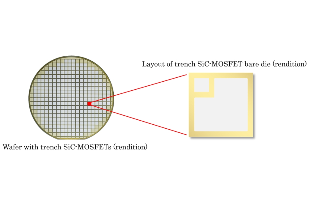
While a hybrid approach combining Si, SiC, and GaN devices is essential for meeting the diverse needs of AI data centers, silicon carbide CoolSiC™ MOSFETs are a critical component in this ecosystem, and in this article, we will discuss their specific applications and benefits in modern power supply unit (PSU) designs.

Figure 2. Server power flow and Infineon Technologies’ comprehensive
product portfolio to address each stage from grid to core in 48V bus
architecture.
The AI revolution is reshaping the design criteria of data center power systems. Unlike conventional server environments that were CPU-centric and operated in relatively predictable load conditions, AI servers operate in highly dynamic states with rapid current surges and higher sustained power demands.
In fact, racks that once consumed under 10 kW are now pushing beyond 300 kW per rack and even above 500 kW in specialized training clusters. SiC based semiconductor solutions are the undisputed choice for such high power rack designs.
And here comes the question – why silicon carbide?
SiC devices are built on a wide bandgap semiconductor material with a bandgap of 3.26 eV—more than three times that of silicon. This physical characteristic provides the following intrinsic advantages for SiC based MOSFET:
• High breakdown field strength allowing for thinner drift regions and thereby reducing specific on-resistance
• High thermal conductivity (3-5x better than Si) improving heat dissipation
• Low switching losses allowing high frequency operation and reducing magnetics size
The low reverse recovery charge (Qrr) of the intrinsic body diode of SiC MOSFET is a decisive differentiator in fast commutation legs, particularly in bridgeless totem pole PFC. The combination of low gate charge (Qg) and reduced output charge (QOSS) broadens zero voltage switching (ZVS) windows in resonant topologies like LLC, enabling operation in the 200–250 kHz range without disproportionate penalties in magnetics or EMI.
From reliability standpoint, SiC MOSFETs exhibit robust avalanche and short circuit capability and a relatively lower positive temperature coefficient of RDS(on) than Silicon MOSFETs. These features simplify current sharing mechanisms in parallel configurations common to multi kilowatt shelves. All these device level benefits align directly with the system level objectives of AI power design: higher efficiency across the load range, smaller and lighter passives, predictable thermal behavior under elevated coolant temperatures, and resilience to abnormal events without compromising on quality and reliability.

Figure 3. Common PFC and LLC topologies addressed with SiC MOSFETs.
From an economic standpoint, SiC enables:
• Smaller power stages and fewer passive components, reducing BOM and footprint
• Higher reliability, minimizing service costs and extending product life
• Superior performance under extreme conditions
The growth of SiC in AI is very well supported by Environmental, Social, and Governance regulations as well as performance and total cost of ownership metrics:
• Hyperscalers like Google, Meta, and Microsoft have set aggressive energy efficiency targets for AI workloads
• Open Compute Project (OCP) standards, such as ORv3, require modular, high-efficiency PSUs
• EU and U.S. energy regulations (e.g. Ecodesign Directive, DOE Level VI) demand stringent efficiency curves across load ranges
• Edge data centers and modular deployments favor compact, high-density designs achievable only with wide bandgap (WBG) semiconductors

Figure 4. 5.5 kW three-phase interleaved LLC converter: reference design and efficiency curve.
This explosive growth poses an immediate and long-term engineering challenge: how to efficiently convert and distribute power from high-voltage AC grid inputs to ultra-low voltage rails (often under 1V) that feed modern AI processors. Moreover, in future, these conversions may happen within space-constrained, thermally stressed environments like liquid-cooled environments.
To meet the current demands of 48V architecture (Figure 2), Infineon Technologies has comprehensive offerings that addresses every node of the power path – from the power grid interface all the way to the processor core. The building blocks of this ecosystem include power switches, gate drivers, controllers, power stages, points of load, and power modules.
With PSUs being at the frontier of power conversion flow in servers, Infineon Technologies’ CoolSiC™ MOSFET families provide the building blocks to support most advanced AI data center architectures.
PSU manufacturers have been widely adopting SiC in Totem Pole Power Factor Correction (TP PFC) designs, where SiC’s fast recovery possible by low Qrr characteristics eliminate the need for slow, lossy boost diodes. Compared to traditional bridged PFC, TP PFC offers 1–1.5% higher peak efficiency in continuous conduction mode (CCM) operation.
The TP PFC stage of the PSU design could involve a 2-level or a 3-level flying capacitor (FC) topology (Figure 3) with or without interleaved approach. 2-level TP PFC is relatively simpler to implement than a 3-level FC design. However, the 3-level FC TP PFC boosts efficiency and density further compared to 2-level approach [2].
In ~400input systems, LLC converters (Figure 3) using SiC MOSFET can operate at up to 500 kHz frequency leading to minimal system loss for the following reasons.
The conduction losses of primary FET are the dominant portion of its overall loss. SiC MOSFET’s relatively lower Rds(on) temperature co-efficient results in relatively lower conduction losses at high temperature operation.
The second dominant loss in the primary FET of LLC is the turn-off loss. SiC MOSFET, being a fast-switching device, enables lower turn-off losses.

Figure 5.Infineon Technologies’ CoolSiC™ MOSFET 400-750V product families.
In addition to the above, the gate driving loss contribution of SiC MOSFET is low due to its lower gate charge compared to Si MOSFETs.
For instance, Infineon Technologies’ 5.5 kW LLC reference design [3] using Gen 2 650V CoolSiC™ MOSFETs in TOLT package achieves almost 99% peak efficiency (Figure 4).
Today Infineon Technologies offers one of the most comprehensive SiC MOSFET offerings in the market and recently has expanded the product families with Generation 2 across 400 V, 650 V, and 750 V voltage classes (Figure 5).
Thus, 400 V CoolSiC™ MOSFET family shows its advantages the best in the multilevel topologies [4]. In 3L Flying Capacitor Continuous Conduction Mode (CCM) Totem Pole topology 400 V SiC provides:
• Lower PFC ripple current leading to lower Root Mean Square (RMS) currents and Total Harmonic Distortion (THD) compared to Triangular Current Mode (TCM) mode.
• Easier control, sensing and electromagnetic interference (EMI) filter design with fixed-frequency operation compared to variable- frequency operation in TCM mode
• Effective frequency on the 3L-PFC inductor is double that of the device switching frequency. Due to the multi-level voltage output of the HF-leg, volt-seconds on the inductor is further reduced. This leads to a potential 4x shrink in PFC-inductor size
• HF-leg switches block half the DC-link voltage, leading to lower switching losses and lower dv/dt swings for a reduced EMI emissions enabling a reduction in the EMI filter size

Figure 6. 650 V CoolSiC™ MOSFET Gen 2 conduction/switching losses in 3.3 kW CCM TP PFC.
650 V CoolSiC™ MOSFET Gen 2 devices (when compared to Gen1) are engineered for higher switching speeds, lower gate charge, reduced reverse recovery charge and output capacitance/charge values [5] — making them ideal for demanding hard-switching topologies (Figure 6). These enhancements directly translate into improved efficiency and thermal behavior.
For hardware design manufacturers, the benefit lies in reduced cooling requirements, greater design freedom, and the ability to hit higher power density targets without compromising on system reliability.
In short, the CoolSiC™ 650V Gen 2 family fits well in the building blocks to support today’s most advanced AI data center power supply architectures encompassing both hard-switching (PFC) and soft-switching (LLC) topologies as described before.
Infineon Technologies’ 750V CoolSiC™ MOSFET portfolio is engineered for higher voltage and harsher operating conditions, making it ideal for both industrial and high-end server PSU applications [6]. Gen 1 MOSFETs offer excellent switching performance and ruggedness, while Gen 2 pushes the performance frontier even further.

Figure 7. 750 V CoolSiC™ MOSFET Gen 2 figures of merit vs 750 V Gen 1.
With RDS(on) values as low as 4 mΩ, these MOSFETs deliver ultra-low conduction losses, essential for efficient high-power systems. Available in through-hole (THD), surface mount device (SMD), as well as SMD top-side cooled (TSC) like Q-DPAK package, this portfolio offers design flexibility.
Gen 2 devices have industry leading lowest specific on-resistance, lower gate charge (QG), output capacitance (QOSS), and output capacitance stored energy (EOSS), translating into faster switching and reduced switching losses. These characteristics are critical for high-frequency, soft-switching topologies where fast transition speeds and minimal dead time improve both efficiency and system density.
Moreover, these devices are being adopted in everything from electric vehicle fast chargers to AI data center PSUs. Their robustness, efficiency, and thermal characteristics are redefining what’s possible at the 8 – 30 kW PSU level.
One of the key features that brings CoolSiC™ Gen 2 on top is the .XT [7] interconnection technology offered across all voltage classes, which marks a significant leap in packaging and thermal performance.
Traditional solder-based interfaces exhibit limitations in thermal resistance and mechanical robustness under high current cycling. The .XT uses a diffusion solder process to create a highly thermally conductive bond between the die and the lead frame. This reduces RthJC (thermal resistance junction-to-case) by up to 25%— significantly enhancing thermal performance and allowing for more compact and reliable system designs.
This advancement is particularly critical in AI data centers where power density is climbing up and thermal margins are shrinking. The .XT also improves reliability under power cycling, reducing the risk of joint fatigue or thermal cracking over time. For system designers, this means longer operational life, less frequent maintenance, and fewer cooling constraints. The powerful combination of CoolSiC™ MOSFETs and.XT technology enables PSUs that are not just smaller and cooler, but also significantly more robust—exactly what’s needed in mission-critical AI infrastructure.
Nowadays environmental impact of power efficiency improvements is often overlooked. However, deploying 650V CoolSiC™ Gen 2 in the PFC stages of all global data centers would save approximately 2.9 terawatt-hours of electricity over five years [1]. That equates to 1.35 million metric tons of CO₂ emissions avoided—the same as removing nearly 300,000 cars from the road.
These calculations are not based on optimistic projections; they are grounded in real operating profiles, mission loads, and validated efficiency gains from production-ready reference boards of Infineon Technologies. As global electricity prices tend to rise with power hungry data centers, and carbon regulation intensifies, these savings become more than a “nice to have”— they are operational imperatives. Today Infineon Technologies helps customers meet Environmental, Social and Corporate Governance targets while also enhancing their bottom line.
Through energy-efficient CoolSiC™ MOSFETs, we contribute to a cleaner, greener digital infrastructure. Sustainability and performance no longer need to be tradeoffs — they go hand in hand.The data centers are no longer a passive utility — it is the active brain of the digital economy. As AI accelerates toward exascale compute, the infrastructure behind it must evolve. Silicon carbide MOSFETs provide the building blocks for that evolution. With unmatched performance in efficiency, density, and reliability, 400V, 650V, and 750V SiC devices are now essential for AI server power conversion stages of the existing 48V and the upcoming 800V or ±400V bus architectures.
Infineon Technologies’ full stack SiC strategy, supported by industry partnerships and deep application expertise, ensures that power electronics keep pace with computing demands. In this new era of power-hungry, thermally constrained, and environmentally conscious compute, the message is clear: AI cannot run without SiC MOSFETs.