FBH develops 200 MHz GaN buck converter module
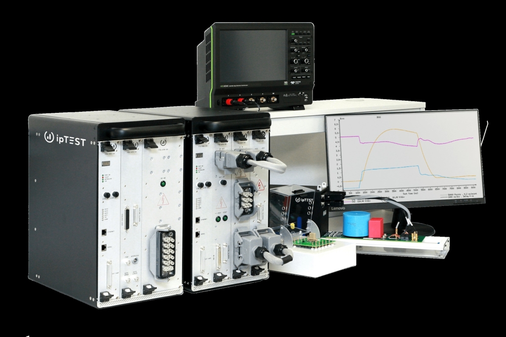
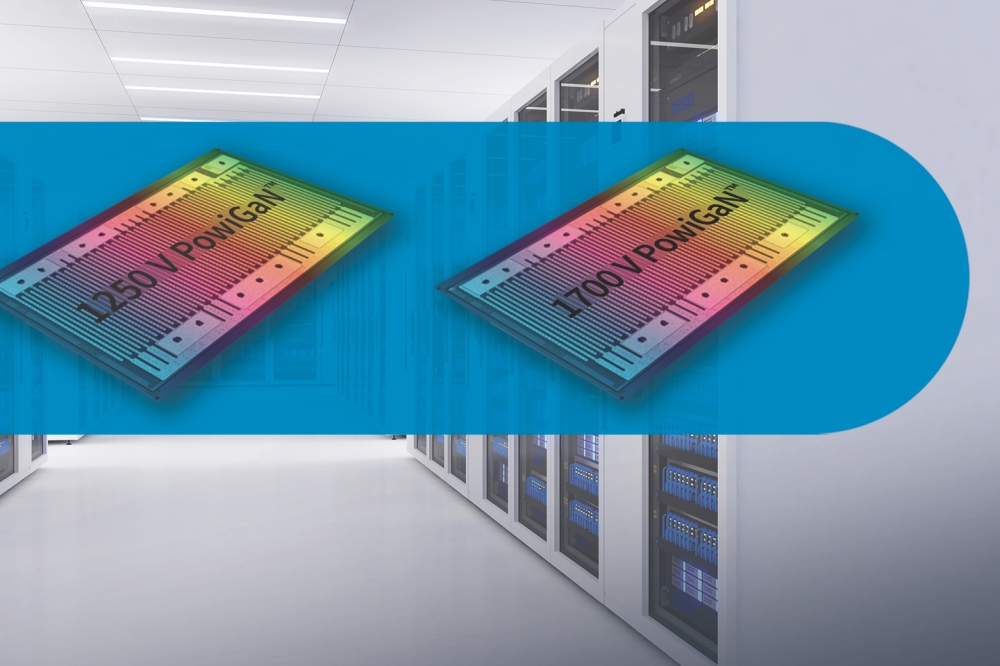
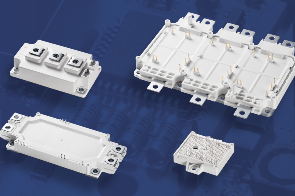
The trend towards ever-larger data centres with much higher energy consumption, is driving a requirement for new power devices. One of the critical components in the distributed power architectures of data centres are the DC/DC (buck) converters to supply the point-of-load (PoL).
To meet these demands, the Berlin-based Ferdinand-Braun-Institut (FBH) has developed a novel, highly efficient and compact GaN-based buck converter operating in the very high frequency (VHF) range up to 200 MHz, which it first discussed in a paper last year at the 54th European Microwave Conference (EuMC) in Paris.
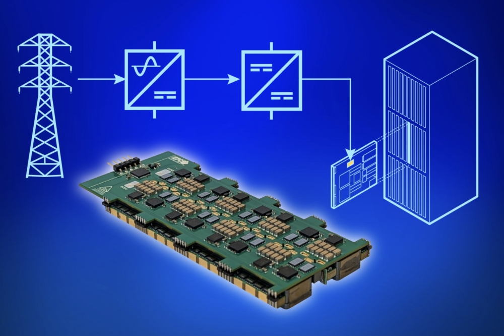
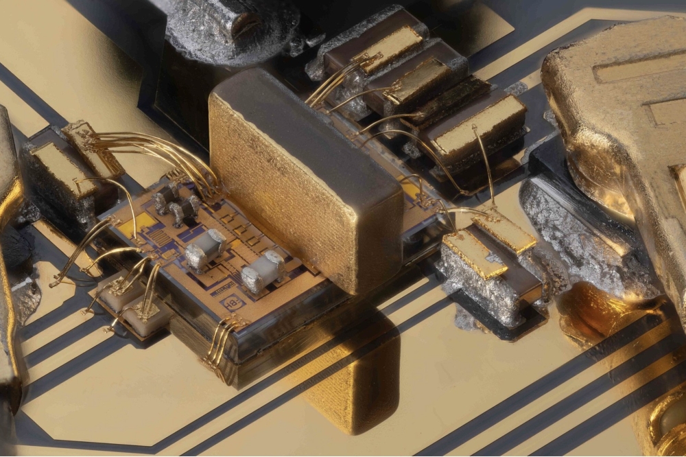
The module includes a GaN half-bridge converter MMIC with integrated drivers, on-chip soldered SMD caps, and inductors to maintain shortest connections. Together with the hybrid low-pass output network (air-core inductor, SMD cap), the chip forms a buck converter with synchronous rectifier for efficient and compact power supply of points-of-load in data centres.
The compact GaN buck converter MMIC (which drives the integrated 10 mm half-bridge power stage GaN-HEMTs) and the hybrid output network are mounted on an AlN single-layer carrier heatsink for optimised power management. Both the GaN chip and the AlN carrier were fabricated in FBH’s cleanroom.
In addition, FBH has introduced new mounting technologies – like 3D integration of a 'capacitor bridge' across the power stage or SMD soldering on the GaN chip to minimise inductive loops – enabling reliable operation at the unusually high frequency of 200 MHz for power converters.
At 200 MHz switching frequency, the buck converter achieves a power conversion efficiency (PCE) up to 71 percent for 32 V DC input voltage (Vdc_in) operation. At 22 W DC output power, an output voltage of 13 V has been reached. At 100 MHz, the PCE peaks at 80 percent for 29 W conversion from 35 V to 14.5 V. For the maximum 38 W conversion to 19 V (48 Vdc_in), the PCE still reaches 75 percent.
Above: Fabricated GaN converter chip in demonstrator with bond-wires and on-chip soldered SMD components; chip area: 2.5 x 1.7 mm2.