Navitas announces support for 800V DC

Navitas Semiconductor, maker of GaNFast GaN and GeneSiC SiC power semiconductors, has announced progress in its development of medium and high 800V DC voltage GaN and SiC power devices to enable the 800V DC power architecture announced by NVIDIA for next-generation AI factory computing platforms.
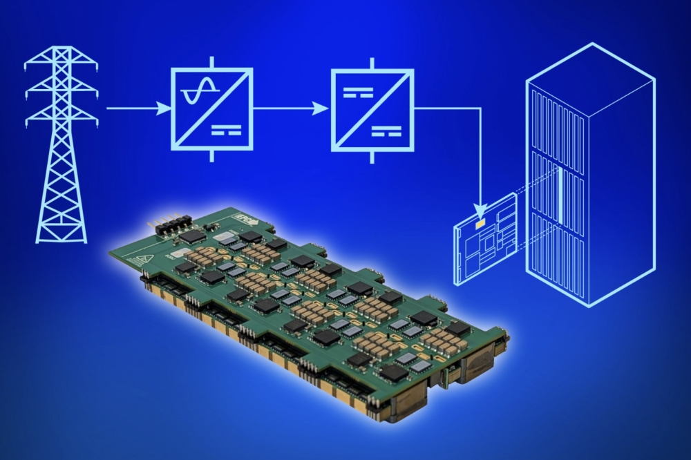
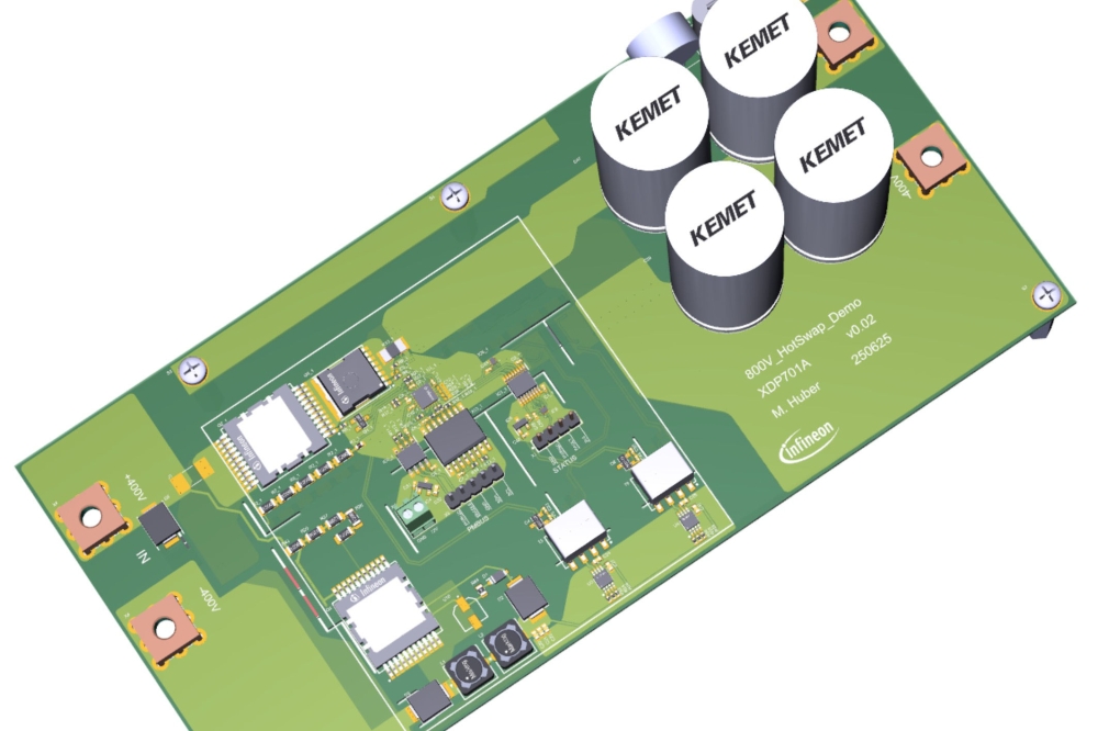
The 800 VDC architecture enables direct conversion from 13.8 kVAC utility power to 800V DC within the data centre power room or perimeter. By using solid-state transformers (SSTs) and industrial-grade rectifiers, this approach eliminates multiple traditional AC/DC and DC/DC conversion stages, maximizing energy efficiency, reducing losses, and improving overall system reliability.
The 800 VDC distribution directly powers IT racks, eliminating the need for additional AC-DC conversion stages, and is stepped down through two high-efficiency DC-DC stages (800 VDC to 54 V/12 VDC, and then to point-of-load GPU voltages), to drive advanced infrastructure such as the NVIDIA Rubin Ultra platform.
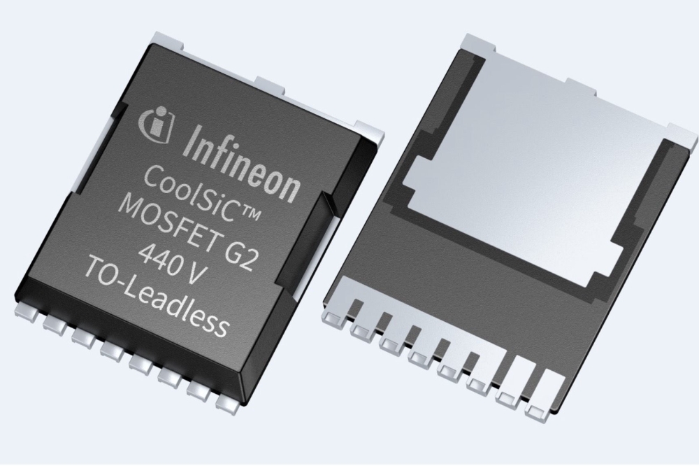
Navitas’ new 100 V GaN FET are optimised for the lower-voltage DC-DC stages on GPU power boards, where ultra-high density and thermal management are critical to meet the demands of next-generation AI compute platforms. Samples, datasheets, and evaluation boards are available for qualified customers.
Additionally, these high efficiency 100V GaN FETs are fabricated on a 200 mm GaN-on-Si process through a new strategic partnership with Power Chip, enabling scalable, high-volume manufacturing.
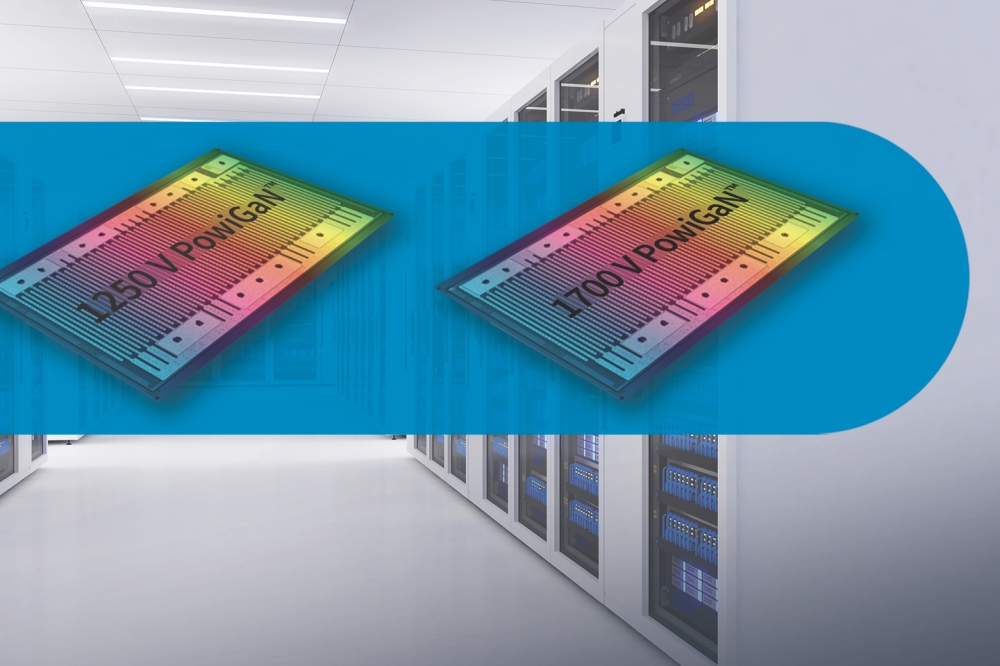
Navitas’ 650V GaN portfolio includes a new line of high-power GaN FETs, alongside GaNSafe power ICs, which integrate control, drive, sensing, and built-in protection features. This ensures exceptional robustness and reliability, supporting the demanding performance and safety requirements of next-generation AI infrastructure.
GaNSafe features ultra-fast short-circuit protection (maximum 350 ns response), 2 kV ESD protection on all pins, elimination of negative gate drive, and programmable slew-rate control. All these features are controlled with 4-pins, allowing the package to be treated like a discrete GaN FET, requiring no VCC pin.
GeneSiC proprietary ‘trench-assisted planar’ provides high performance over temperature, delivering high-speed, cool-running operation for high-power, high-reliability applications. GeneSiC technology offers a broad voltage range, stretching from 650 V to 6,500 V and has been implemented in multiple megawatt-scale energy storage and grid-tied inverter projects, including collaborations with the US Department of Energy (DoE).
Chris Allexandre, president and CEO of Navitas said: “Navitas is undergoing a fundamental transformation, driven by the convergence of GaN and SiC technologies to power the world’s most advanced systems. From grid to GPU, our focus now extends far beyond mobile, as we address the megawatt-scale demands of AI factories, smart energy infrastructure, and industrial platforms with differentiated, high-performance power solutions.”