Advancing SiC substrate and epitaxial technologies for next-generation power devices
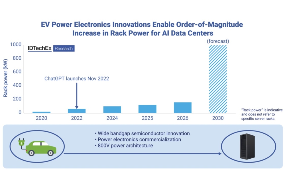
Silicon carbide is rapidly reshaping next-generation power electronics, but the real performance gains depend on advances in substrate and epitaxial material quality that improve yield, efficiency and reliability at scale. As the industry moves toward 200 mm wafers and higher-voltage applications, material engineering is becoming central to the future economics of SiC power devices.
BY Gary Ruland, Rajan Rengarajan, Shanthi Subramanian, Qi Yang, Ilya Zwieback Coherent Corp
The power electronics inflection point
Over the past decade, the SiC power device market has transitioned from a specialty niche to a mainstream enabling technology. The full promise of SiC — lower switching losses, higher operating temperatures, higher breakdown voltages, and smaller form factors1 — depends on continued advances in substrate and epitaxial quality. The progress in the upstream materials is central to industry success.
Why substrate quality defines device performance
A SiC power device begins its life as a boule of single-crystal 4H-SiC, grown by Physical Vapor Transport (PVT) at temperatures exceeding 2,200°C. The resulting ingot is sliced into substrates that serve as the foundation for epitaxial growth. Every defect present in the substrate — whether a micropipe, threading screw dislocation (TSD), basal plane dislocation (BPD), or stacking fault — has the potential to propagate into the epitaxial layer and compromise device reliability, yield, and forward voltage stability.
Micropipes, hollow core screw dislocations, are device killers. Once present in SiC at densities of tens per cm2, they have been virtually eliminated in commercial substrates through advances in seed preparation, vapor phase control, and thermal gradient engineering. Today’s Coherent commercial 150 mm substrates show typical micropipe densities below 0.05 cm-2. The focus has now shifted to subtler but equally consequential defect classes – BPD and TSD dislocations.

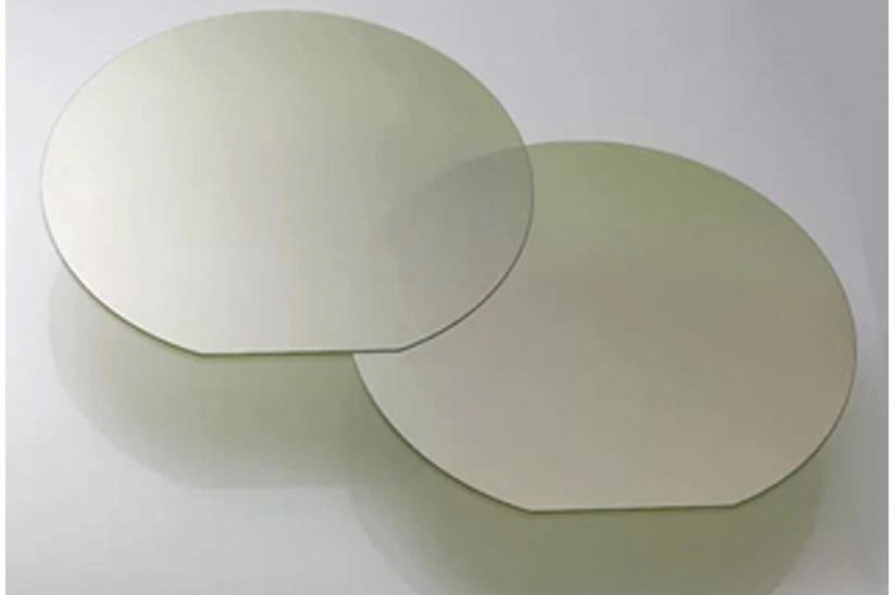
SiC substrate wafer — 150mm SiC Substrate
BPDs in Coherent substrates remain the most prevalent structural defects, present at typical densities of 500 cm-2. During epitaxial growth, some BPDs penetrate from the substrate into the epi in the active device area. Under bias, BPDs dissociate into Shockley Stacking Faults (SSF). As these SSFs grow and expand through the active device area, they act as resistive barriers causing increase in on-resistance and forward voltage and leading to local overheating and device degradation.
In Coherent’s production substrates, TSDs are found in typical densities of 300 cm-2. They generate local regions of high electric field around their cores leading to micro-leakages under reverse bias. The micro-leakages contribute to the overall leakage current of the device and reduce the breakdown voltage.
The transition from 150 mm to 200 mm substrates, now underway across the industry, amplifies these challenges. Larger diameter wafers require tighter control of thermal gradients during growth to avoid lattice curvature, wafer bow and dislocation multiplication. Achieving uniform dislocation density and resistivity across a 200 mm substrate is an engineering challenge that requires simultaneous advances in crystal growth hardware, seed preparation, and tight in-growth process control.
Epitaxial growth: where device performance Is born
If the substrate defines the defect floor, the epitaxial layer defines device performance. Chemical Vapor Deposition (CVD) of 4H-SiC epitaxial layers on polished substrates enables precise control of doping concentration and layer thickness — parameters that directly determine the breakdown voltage, on-resistance, and switching behavior of the finished device.
For a 1,200 V power MOSFET, the typical drift layer thickness for Coherent epitaxial wafer a is ~ 10– μm with a net n-type doping of ~1× 10¹6 cm-3. Typical thickness uniformity is < 3% and doping uniformity < 6%. For 3,300 V devices targeting traction applications, drift layer thicknesses extend to 30–35 μm with correspondingly lower doping levels approaching 3 × 10¹⁵ cm-3. Maintaining uniformity at these thicknesses while suppressing epitaxial defects, such as in-grown stacking faults and inclusions, requires precise control of growth chemistry, surface preparation, and reactor design. Defect density of < 0.5/cm2 are routinely achieved through Epi growth process optimization and improvement in substrate quality.
BPD conversion efficiency — the fraction of substrate BPDs that convert to the less-harmful threading edge dislocation (TED) configuration during epitaxial growth — has become a key industry benchmark. Through deliberate miscut angle optimization (typically 4° off-axis toward [11-20]) and controlled off-axis growth conditions, conversion efficiencies above 99% are achievable, dramatically reducing the density of BPDs in the active device layer.
For device manufacturers, these numbers carry direct yield implications. At a hypothetical 1200 V MOSFET die size of 7 mm², an epitaxial defect density of 1 cm-2 produces a statistical first-pass yield ceiling below 93% before process losses are factored in. Reducing that density to 0.3 cm-2 pushes the ceiling above 98% — a difference that potentially demarcates profitability at automotive volumes.
The economics and scale-up imperative
Material quality improvements are only meaningful if they can be delivered at the volumes and cost points the market demands. This is where the real competitive differentiation in the SiC supply chain is taking shape.
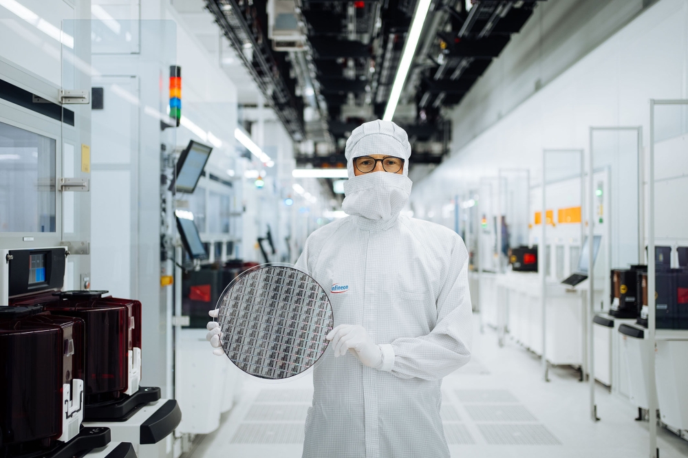
The automotive sector alone — driven by EV powertrain electrification — is expected to consume hundreds of millions of SiC MOSFETs annually by the end of this decade. Meeting this demand requires not just larger substrates, but higher substrate-to-device yield, and that yield is predominantly a function of epitaxial defect density with targets now approaching <0.05/cm2. This creates a clear strategic imperative: the integration of highthroughput, in-line defect inspection with closed-loop feedback to epitaxial process control. Photoluminescence (PL) mapping, X-ray topography, and automated optical inspection tools capable of classifying defect types across full 150 mm and 200 mm wafers are becoming standard in high-volume manufacturing environments. Machine learning-assisted classification of defect signatures is accelerating the speed at which process deviations are detected and corrected.

Cross-section schematic of SiC epitaxial layer stack showing substrate, buffer, and drift layer
Simultaneously, the industry is investing in substrate supply security. Vertically integrated supply chains — in which substrate crystal growth, wafering, CMP polishing, epitaxial deposition, and device fabrication are managed within a single organization or through deeply committed supply partnerships — offer advantages in quality feedback loops that are difficult to replicate in fully disaggregated models. The ability to trace a device yield excursion back to a specific boule, growth run, or polishing batch is only possible when data flows freely across the supply chain.
Emerging device structures and their material requirements
Next-generation SiC device architectures are placing even more demanding requirements on substrate and epitaxial quality. SiC trench MOSFETs have been developed to reduce the conduction and switching losses of the traditional planar MOSFET. Trench MOSFET has a lower ON-resistance, which reduces the energy lost as heat and allows for smaller device footprint. A small chip area has low parasitic capacitances, which allows for faster switching.

(a) SICA Defect map: >97% 5mmx5mm Total usable area achieved. (b) SICA image of killer defect : polytype inclusion

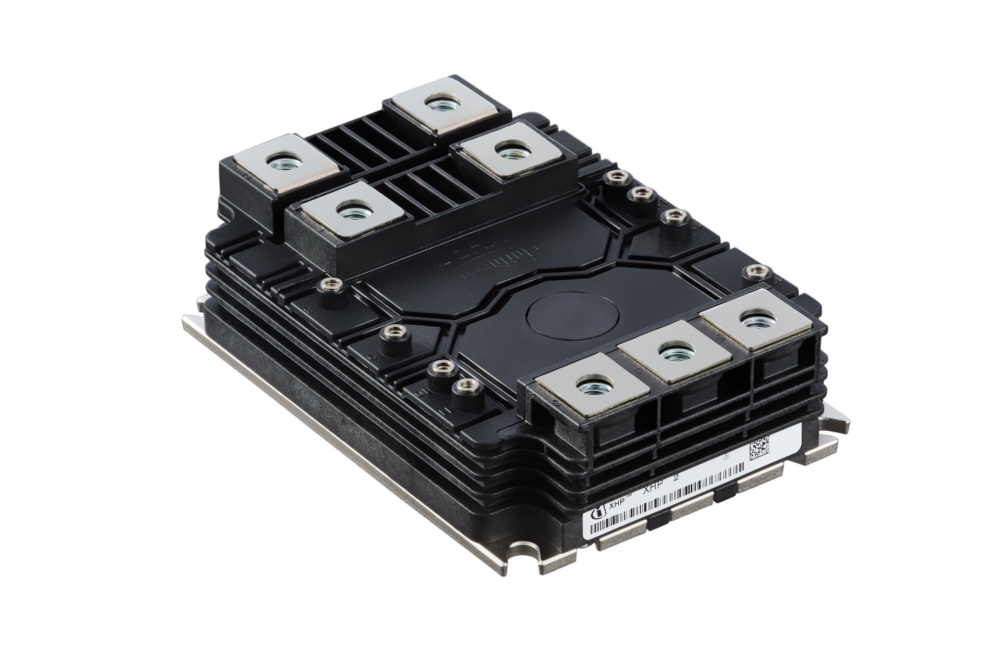
SiC Module
High-voltage applications above 3,300 V — including solid-state circuit breakers, HVDC conversion, and next-generation traction drives — demand epitaxial layers exceeding 40– 50 μm in thickness with exceedingly tight doping uniformity. At these thicknesses, managing parasitic stress and maintaining step-flow growth morphology across the entire wafer area becomes a significant engineering challenge. Graded buffer layers and strainengineered epitaxial stacks are being explored to manage this challenge without sacrificing the electrical properties of the drift region.
In addition to MOSFETs, there are other SiC devices under development, such as Insulated Gate Bipolar Transistor (IGBT) and Bipolar Junction Transistor (BJT). Fundamentally, operation of both IGBT and BJT is based on injection of the minority carriers. In IGBT, this leads to a very low ON-resistance of the drift region under a high bias up to 20 kV. In BJT, this improves the reliability of the transistor operation under high voltage and at elevated temperatures. SiC BJTs showed the lowest ON-resistance in a broad temperature range. Due to the variety of technological, material and device issues, neither IGBTs nor BJTs entered the commercial SiC device mainstream.
Material requirements for IGBTs and BJTs are different than those applied to MOFETs. IGBT requires precisely doped (~2e14 cm-3) ultra-thick (up to 200µm) epilayer having high carrier lifetime (5-20 µs). The most common n-channel IGBT design requires a p-type substrate, which is a challenge. An alternative IGBT design utilizes an n-type substrate on which a thick n-type drift and p-type “cap” epilayers are grown. This is also a challenge. IGBT design may require carbon ion implantation to annihilate carbon vacancies, which are lifetime killers.
BJT design requires precise, heavily doped multiple epilayers with abrupt doping profiles for transistor base, emitter and collector. The lifetime in the BJT drift layer must be tightly controlled. Both IGBT and BJT are susceptible to bipolar degradation caused by BPDs.
In order to bring IGBT and BJT into the commercial SiC device mainstream, significant progress must be achieved to solve the related material and device design issues.
Looking ahead: the path to 200 mm and beyond
The transition to 200 mm SiC substrates is the defining challenge and opportunity for the materials community over the next three to five years. At 200 mm, the cost per unit area of SiC substrate decreases substantially, and the number of dies per wafer increases by approximately 78% compared to 150 mm — a step change in economics that will be critical to enabling SiC’s penetration into mid-range EV platforms and industrial applications where cost sensitivity is higher.
Achieving this transition at production scale requires overcoming wafer bow and warp issues that emerge at larger diameters, developing CMP processes that maintain surface roughness specifications (Ra < 0.5 nm) across the full 200 mm area, and qualifying epitaxial reactor platforms capable of delivering the same defect density and uniformity performance achieved on 150 mm wafers. Early production results from leading substrate suppliers are encouraging, but achieving the consistent, high-yield 200 mm substrate supply that device manufacturers will require is still an active engineering effort.
Beyond 200 mm, the long-term roadmap envisions continued improvements in dislocation density, the broader adoption of nitrogen and aluminum co-doping strategies to improve substrate conductivity uniformity, and deeper integration of AI-driven process control across the entire substrate and epitaxial manufacturing sequence. The physics of SiC crystal growth will continue to set limits, but the engineering systems surrounding those physical processes have enormous room to improve.
Conclusion
Silicon carbide is no longer an emerging technology — it is the power electronics platform of the energy transition. The performance, reliability, and cost trajectory of SiC power devices is inseparably linked to the quality of the substrate and epitaxial materials from which they are built. The progress achieved over the past decade in reducing micropipe density, improving BPD conversion efficiency, and delivering uniform, low-defect epitaxial layers at 150 mm scale has been remarkable. The challenge ahead — scaling those achievements to 200 mm, reducing defect densities further, and enabling next-generation device architectures — is equally ambitious.
The organizations that lead this materials challenge will define the competitive landscape of SiC power electronics for the decade ahead. For the industry as a whole, the continued investment in substrate and epitaxial technology is not a cost of doing business — it is laying the cornerstones that support the most important power electronics revolution of this generation.
Gary Ruland is a technology executive at Coherent. With a PhD in physical chemistry and decades of experience in advanced materials, he is a recognized thought leader in SiC substrate and epitaxial technology for power electronics applications.
Rajan Rengarajan is a Senior Director at Coherent, leading SiC crystal growth and wafering R&D. With a PhD in crystal growth and deep expertise in developing advanced ferroelectric and wide-bandgap materials, his focus has been on SiC materials and technologies for the past two decades.
Shanthi Subramanian is a Senior Director at Coherent, leading SiC metrology and epitaxy R&D. She holds a PhD in materials science and engineering, brings more than 25 years of experience, driving innovation across crystal growth, process development, and metrology.
Qi Yang is a Senior Manager at Coherent, leading SiC data systems. With a PhD in experimental condensed matter physics, his work at Coherent brings software, data, and AI technologies to SiC manufacturing.
Ilya Zwieback is a Senior Director at Coherent. With a PhD in semiconductor materials and devices, and deep experience in crystal growth, epitaxy, and devices of a wide range of semiconductors, he has been a key contributor to SiC technology for the past two decades.