Minding the ultra-wide bandgap – gearing up for Gallium Oxide
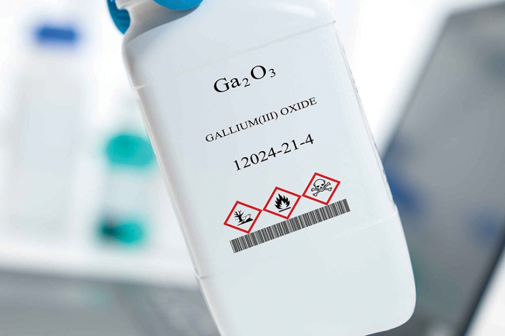
Minding the ultra-wide bandgap – gearing up for Gallium Oxide
As AI infrastructure, electrified transport and renewable energy systems drive demand for higher-voltage, higher-efficiency power conversion, gallium oxide is emerging as a serious contender in the next generation of ultra-wide bandgap semiconductors. Once viewed as a long-term research material, gallium oxide is now moving rapidly toward industrial deployment, promising new levels of performance, scalability and cost efficiency in applications beyond the reach of today’s silicon carbide and gallium nitride technologies.
For much of the last decade, the power electronics industry has been dominated by discussions around silicon carbide and gallium nitride. Both materials have transformed expectations surrounding efficiency, switching speeds and power density, enabling major advances across electric vehicles, renewable energy systems, industrial automation and data centre infrastructure. Yet even as silicon carbide and gallium nitride continue their expansion into mainstream markets, attention is already shifting toward what many now see as the next major breakthrough material for high-voltage power electronics: gallium oxide.
Until recently, gallium oxide remained largely confined to research laboratories and academic discussions. Although engineers and scientists recognised its impressive electrical properties many years ago, there was widespread scepticism about whether the material could ever be manufactured economically at scale. Today, however, that perception is changing rapidly. A combination of mounting market demand, improvements in manufacturing pathways and the unprecedented rise of AI-driven power consumption is accelerating interest in gallium oxide across the semiconductor industry.
What makes the timing particularly significant is that the wider power electronics landscape itself is evolving. Electrification trends have already pushed operating voltages higher across multiple industries. Electric vehicles have moved from 400V to 800V architectures in pursuit of faster charging and improved efficiency, while renewable energy systems increasingly require more advanced power conversion technologies capable of handling greater loads with minimal losses. At the same time, hyperscale AI infrastructure is creating entirely new power delivery challenges inside modern data centres, where operators are now discussing the possibility of bringing hundreds of volts — and eventually even kilovolt-level power distribution — directly onto server motherboards.
These trends are forcing the industry to look beyond the capabilities of existing semiconductor materials. While silicon carbide and gallium nitride remain highly effective in many applications, the move toward ultra-high-voltage power conversion is creating demand for materials capable of operating more efficiently at significantly higher electric fields. This is where gallium oxide begins to stand apart.
Gallium oxide belongs to the category of ultra-wide bandgap semiconductors. Its bandgap is approximately 4.9 electron volts, substantially wider than the roughly 3.2 to 3.3 electron volt bandgaps associated with silicon carbide and gallium nitride. Although this may appear to be a modest numerical difference, the implications for device performance are considerable. A wider bandgap enables semiconductor devices to tolerate much higher electric fields before breakdown occurs, allowing engineers to design smaller, faster and more efficient devices capable of operating at far higher voltages.
The practical significance of this becomes clearer when examining the changing nature of modern power architectures. Historically, many power conversion systems operated at relatively modest voltages, particularly in battery-driven and distributed electronic systems. However, as industries seek greater efficiency and lower transmission losses, higher voltages are being pushed progressively closer to end-use applications. Data centres are perhaps the clearest example of this transformation. Just a few years ago, server-level power architectures centred largely around 48V distribution. Today, some of the world’s largest AI infrastructure providers are discussing 800V distribution schemes inside computing systems, with long-term ambitions extending even further.
Higher voltages reduce current requirements and improve overall efficiency, but they also place enormous demands on power semiconductors. Devices must not only tolerate these voltages safely, but also maintain compact form factors and minimise thermal losses. Gallium oxide’s electrical properties position it as a potentially transformative solution for these emerging requirements.
Importantly, gallium oxide is not simply viewed as a replacement for existing technologies. Instead, many experts believe it could open entirely new application domains for semiconductor-based power conversion. One area receiving particular attention is grid infrastructure. Traditional electrical grids still rely heavily on large oil-filled transformers and mechanical power conversion systems that are expensive, maintenance-intensive and physically cumbersome. As the energy transition accelerates, there is growing interest in replacing portions of this legacy infrastructure with solid-state transformers and advanced semiconductor-based conversion systems capable of operating directly at much higher voltages.
This is precisely the type of environment where gallium oxide could offer major advantages. Its ability to operate efficiently in kilovolt-level applications could enable entirely new approaches to power conversion across grid infrastructure, renewable energy systems and industrial power distribution. In electric vehicles, meanwhile, the ongoing shift toward higher-voltage architectures may eventually create further opportunities for gallium oxide devices, particularly as manufacturers continue pursuing improvements in charging speed, efficiency and power density.
Yet one of the most significant reasons for growing excitement around gallium oxide lies not only in its electrical performance, but also in its potential manufacturability. Historically, many promising semiconductor materials have failed to achieve widespread commercial success because they proved too difficult or expensive to produce at scale. Silicon carbide itself continues to face substantial manufacturing challenges, particularly in the production of large-diameter wafers with sufficiently low defect densities for high-volume device fabrication.
Gallium oxide, by contrast, offers a potentially more scalable production pathway. One of its key advantages is that it can be grown using melt-based crystal growth methods that resemble traditional silicon manufacturing techniques more closely than silicon carbide production processes do. This compatibility with established semiconductor infrastructure could prove decisive in accelerating commercial adoption.
The semiconductor industry has spent decades building highly optimised manufacturing ecosystems around large-format wafers, particularly 200mm and 300mm platforms. Fabrication equipment, lithography systems, deposition tools and process technologies have all evolved around these standards. Gallium oxide’s compatibility with such infrastructure means the industry may be able to leverage much of its existing manufacturing base rather than requiring entirely new production ecosystems.
This could dramatically reduce both cost and complexity. Larger wafers enable more devices to be manufactured per substrate, improving equipment utilisation and lowering the cost per chip. In silicon carbide manufacturing, achieving defect-free 300mm wafers remains a major technical challenge. Gallium oxide, however, appears to offer a more straightforward route toward large-diameter substrates, potentially giving it a significant long-term economic advantage.
The existence of mature manufacturing equipment is also highly important. Much of the infrastructure required to process gallium oxide devices already exists within semiconductor fabrication facilities. Physical vapour deposition, chemical vapour deposition, lithography and related technologies are already widely deployed across advanced semiconductor manufacturing. If gallium oxide substrates can be produced reliably at scale, many elements of the industrial ecosystem are effectively ready to support them.
Physical vapour deposition technologies, in particular, are expected to play a major role in unlocking the full potential of gallium oxide devices. Although the material offers exceptional electrical properties, it also presents one important challenge: relatively poor thermal conductivity. Compared with silicon carbide, gallium oxide conducts heat far less efficiently, creating potential concerns around heat dissipation in high-power applications.
Thermal management has become one of the defining engineering challenges across the semiconductor industry, extending far beyond power electronics alone. AI processors, GPUs and high-bandwidth memory systems are all generating unprecedented thermal loads, forcing engineers to develop increasingly sophisticated cooling and packaging strategies. This broader industry effort may ultimately benefit gallium oxide significantly.
Experts point out that the semiconductor sector already possesses many of the tools required to address thermal limitations. Advanced packaging technologies, thermally conductive metallisation layers, wafer thinning techniques and engineered interfaces are all areas where substantial progress is being made. Physical vapour deposition processes are expected to contribute heavily in this area by enabling highly controlled interfaces, advanced contact structures, passivation layers and thermal management coatings.
Interestingly, this is creating a convergence between previously separate areas of semiconductor development. Historically, the world of advanced logic and memory packaging evolved largely independently from power semiconductor manufacturing. Today, however, many of the same packaging concepts developed for high-performance computing are becoming increasingly relevant to next-generation power electronics.
This convergence is one of the most striking features of the current semiconductor landscape. As industries push simultaneously toward higher performance, greater efficiency and increased miniaturisation, technologies developed in one sector are rapidly finding applications in others. The challenges facing AI processors and advanced power semiconductors increasingly overlap, particularly in the areas of thermal management, packaging density and power delivery.
For many industry observers, this broader technological convergence is helping accelerate gallium oxide’s path toward commercialisation. Rather than requiring entirely new inventions, the material may benefit from innovations already occurring elsewhere in the semiconductor ecosystem.
That acceleration is also reflected in changing industry perceptions. Only a short time ago, many semiconductor manufacturers viewed gallium oxide as a technology that remained at least a decade away from practical deployment. Today, however, the conversation has shifted noticeably. Companies are actively evaluating how ultra-wide bandgap semiconductors might fit into future product strategies, driven largely by the growing demands of AI infrastructure, grid modernisation and electrified transportation.
As a result, gallium oxide now appears to be transitioning from a purely academic topic into the early stages of industrial deployment. Initial commercial devices could emerge within the next few years, while broader high-volume manufacturing may follow later in the decade if substrate scaling and packaging challenges continue progressing successfully.
Despite the excitement, few experts expect gallium oxide to replace silicon carbide or gallium nitride entirely. Instead, the future power electronics landscape is likely to become increasingly diversified, with multiple semiconductor materials serving different operating ranges and application domains. Silicon carbide and gallium nitride will continue playing vital roles in many voltage classes, while gallium oxide is expected to establish itself primarily in the highest-voltage applications where its unique properties offer the greatest advantages.
In some areas, particularly at the upper end of the voltage spectrum, gallium oxide may eventually displace portions of the silicon carbide market, especially if its manufacturing economics prove superior at scale. However, the more likely scenario is one of coexistence rather than outright disruption. Future power architectures may increasingly incorporate multiple semiconductor materials across different stages of energy conversion, from the electrical grid all the way down to processors and edge devices.
What is becoming increasingly clear is that semiconductor innovation cycles themselves are accelerating dramatically. Technologies once expected to require decades to commercialise are now advancing far more quickly, driven by the strategic importance of semiconductors across nearly every major industry. AI, electrification and the global energy transition are all intensifying pressure for faster innovation and deployment.
Gallium oxide is emerging at exactly the moment when the industry needs new solutions for ultra-high-voltage power conversion. While significant engineering challenges remain, the combination of compelling electrical performance, scalable manufacturing potential and strong market demand is pushing the material rapidly toward commercial reality.
The next chapter in power electronics may therefore extend beyond silicon carbide and gallium nitride sooner than many expected. Increasingly, gallium oxide appears poised to become one of the defining semiconductor materials of the high-voltage era.