Running in the right direction with 48V for AI processor power

As AI processors demand ever-higher power levels, power delivery efficiency is becoming a critical challenge for AI infrastructure. This article explores how 48V Factorized Power Architecture can significantly reduce energy losses, lower operational costs and improve scalability compared with conventional 6V multiphase power delivery approaches in next-generation AI data centres.
By Maury Wood VP Strategic Marketing Vicor Corporation
At a certain level of abstraction, modern AI processors simply exchange trillions of bytes of data per second with other AI system processors (typically CPUs), network processors and memory devices, perform quadrillions of parallel vector operations per second, and thermally dissipate two to three thousand watts continuously, around the clock, every day of the year. From that perspective AI processors are the world’s most expensive electric heaters. Indeed, a single contemporary AI GPU plus high-bandwidth memory (HBM) accelerator continuously dissipates the same amount of heat as a salon-type hair blow dryer. AI power system engineers are hyper-focused on efficiently supplying the required electrical energy while reducing the thermal dissipation caused by delivering sufficient power to these massive compute engines. The recent shift to an 800VDC based data center rack feed is gaining momentum as the AI infrastructure industry’s next move, following the shift away from 12V power delivery networks (PDNs) to more efficient 48V PDNs. However, challenges with voltage regulator current density and current gain at the point of load is causing the industry to head in the wrong direction. This shift away from efficient 48V PDNs and back to 6V and 2V PDNs requires the management of huge and unnecessary thermal power losses.
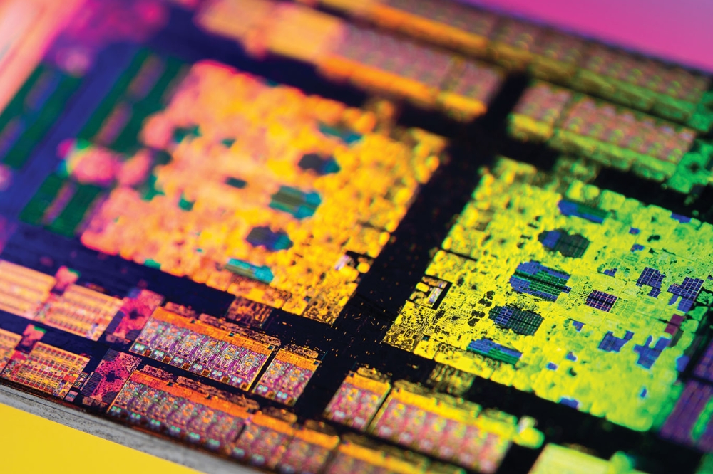
A state-of-the-art AI processor (Figure 1) with a thermal design power (TDP) of 3kW, requires 5,000 amps thermal design current (TDC) at 0.6VDD. Note that AI processors can have dozens of supply rails with different voltage and current delivery demands, so the modeling in this article is simplified for clarity. The package dimensions for this chiplet based AI processor example are assumed to be about 55mm by 74mm, or about 4,070mm2. This yields a package-level (typically CoWoS or EMIB) power density of about 740mW/mm2 and a current density of about 1.23A/mm2, supporting the notion of these processors as fierce heaters requiring direct-to-chip liquid cooling to operate continuously and reliably over a period of years.

Figure 1. Example state-of-the art AI processor, with CoWoS chiplet package dimensions 55mm by 74mm, or 4,070mm2 area
The proposed Industry-standard power delivery architecture: Running in the wrong direction
The legacy standard point-of-load (PoL) AI processor power delivery architecture, whether laterally-placed (LPD) or vertically-placed (VPD), uses interleaved pulse-width modulated (PWM) trans-inductor voltage regulators (TLVRs), typically with dozens of vertically-placed power modules controlled in sequential “multiphase” outputs. Numerous multiphase VRs are combined to meet the current (both continuous and peak) demands of the various supply rails (multiple logic core rails, HBM memory rails, physical layer SerDes rails, input and output rails and others). In this power architecture, the digital multiphase controller must achieve analog voltage averaging across phases within the processor voltage ripple tolerance, as well as manage accurate output current sharing among the dozens of PoL multiphase power modules.

Figure 2. 6V multiphase powertrain showing transformation then regulation stages and the voltage averaging characteristic
A key technical characteristic of the multiphase architecture is a powertrain structure that performs voltage transformation followed by voltage regulation. In the context of an AI accelerator card with a 48V input voltage, the first stage of the powertrain, transforms 48V to 12V (4-to-1 fixed-ratio conversion) or more recently and commonly 48V to 6V (8-to-1 fixed-ratio). The second stage, a multiphase TLVR buck regulator, regulates 6V to sub-1V levels, for example 0.6V (10-to-1 buck down) for the processor core rail. The initial transformation stage is commonly referred to as an intermediate bus converter (IBC), and the bus that conducts between stages is commonly referred to as the intermediate bus. Due the very high input current requirements of state-of-the-art AI processors (such as the 5kA TDC at 0.6V used for the analysis in this article), the current across the 6V intermediate bus is 500A. Assuming 200 micro Ohms (mΩ) of PCB power and ground plane lumped resistance across this lateral intermediate bus, the I2R thermal loss is 50W for each AI accelerator card, of which there are dozens in a rack.
The proposed future AI data center architecture is based on 800V power distribution and will rely on separate “sidecar” power racks, creating an intermediate bus, currently proposed to be 6V, to the compute rack processor trays which then feed the multiphase VRs. This power architecture suffers huge intermediate bus PCB thermal losses as the PDN impedance is significantly higher than 200mΩ), and drives the need for silver-plated copper bus bar liquid cooling, and faces critical metal cost and sourcing challenges.

Figure 3. Current industry-standard 6V multiphase power architecture with high intermediate bus power and scalability constraints
Running in the right direction: 48V Factorized Power Architecture with current multiplication:
The high performance alternative to multiphase TLVR voltage regulation is 48V Factorized Power Architecture (FPA™), using current multiplication at the PoL. This power architecture extends 48V from the AI accelerator input power connector to the AI processor, dramatically reducing thermal losses in AI compute trays and AI factories as compared to the 6V multiphase VR and intermediate bus power architecture.
FPA uses two DC-DC converter stages, but architected as voltage regulation followed by voltage transformation, the reverse of the standard multiphase VR powertrain architecture. The regulation stage is implemented with a buck-boost or buck DC-DC converter. The transformation stage is implemented with a current multiplier, which divides the regulated 48V factorized bus by a K factor, in this example K = 48, which yields a 1V nominal AI processor supply rail. The inverse of the K factor is the current gain of the voltage transformation stage.
Current multipliers possess unique and innovative high performance characteristics including:
· Ideal DC-DC transformer behavior with no internal energy storage
· High current gain, >40 and high current density >3A/mm2 continuous and 6A/mm2 peak
· Low output impedance
· High bandwidth to enhance transient response agility
· Best-in-class 8.6A/ms transient response, with 400ns slew rate
· Low EMI with a clean noise spectrum attributable to zero-voltage switching (ZVS) and zero-current switching (ZCS) technology
· Low output voltage ripple
· Module thermal resistance of less than 0.15°C/W
· 1.5mm module height
Running in the right direction, 48V FPA to the PoL dissipates 64 times less heat on the intermediate / factorized bus compared to the 6V multiphase VR power architecture, and 576 times less compared to emerging 2V integrated voltage regulator (IVR) solutions.
Using the exemplary state-of-the-art 3kW TDP and 5kA TDC AI processor, assuming a 200mΩ intermediate / factorized PCB power and ground plane bus resistance, 48V FPA thermally dissipates about 780mW on the factorized bus, while 6V multiphase solutions thermally dissipate about 50W on the intermediate bus.

Figure 4. Industry standard multiphase VPD versus Factorized Power Architecture VPD illustrates the 64 times higher intermediate bus thermal dissipation compared to 48V FPA VPD. Both approaches assume 200µΩ bus resistance. Simplified models shown.
Aggregate energy and cost savings – 48V to the PoL versus 6V to the PoL at the AI factory level
Summarizing the key point, the 6V multiphase power architecture dissipates 64 times more heat compared to the 48V factorized power architecture. While 800V distribution to AI sidecar power racks is reducing thermal losses, 6V PDNs for multiphase VR power architectures are increasing intermediate bus thermal losses by 64x. It seems clear the 6V multiphase AI processor power architecture is running in the wrong direction with respect to the pressing industry and broader societal desire to decrease AI factory energy usage.
The bottom line is the bottom line

Figure 5. Intermediate bus thermal power reduction – Vicor 48V FPA versus 12V multiphase, 6V multiphase, and 2V integrated voltage regulation
Frontier AI factories, on the path to 1GW compute capacity, use as many or more than 250,000 GPUs. GPUs are on track to consume 50% of the total utility energy delivered to AI factories of the future. The aggregate 6V multiphase voltage regulator intermediate bus thermal loss for 250,000 GPUs (using the 3kW TDP per GPU model processor) is about 12.5MW (megawatts), while the corresponding aggregate 48V factorized bus thermal loss is about 195kW (kilowatts). This 64x reduction factor equates to about 12.3MW, or about 108GWh (gigawatt-hours) annually. Again, these processors operate 24 hours a day, 365 days per year. Assuming $45,000 per 1GWh for wholesale utility-scale electricity, a 109GWh reduction equates to about $4.9M (million) USD OPEX reduction per year. Over a four-year depreciation period, the aggregate OPEX reduction nears $20M.
In summary, the $5M saved annually in a 1GW AI factory electrical OPEX, plus the 55W of reduced heat losses per GPU enabled through the use of 48V to the PoL as compared to the 6V multiphase power architecture, make evident that 48V-based factorized power architecture is running in the right direction, with respect to performance, operational cost, and power savings in the AI infrastructure of the future.
FPA™ is a trademark of Vicor Corporation.