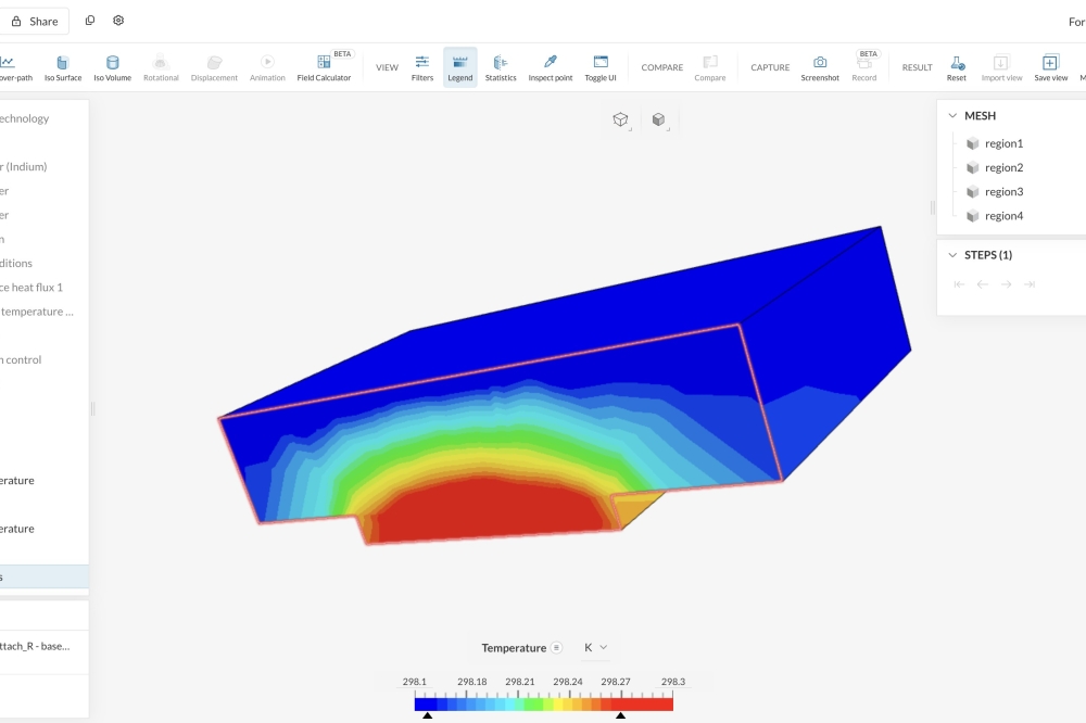
Navitas introduces new package for HV SiC MOSFETs
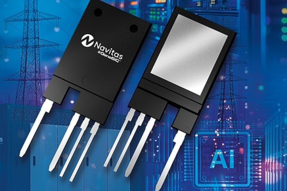
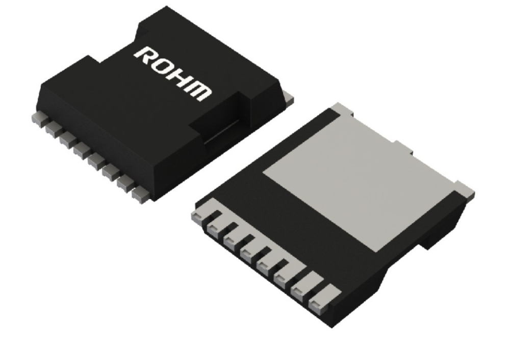
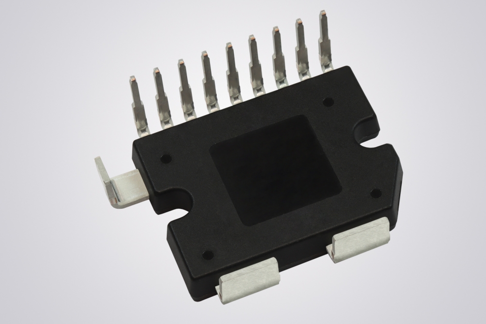
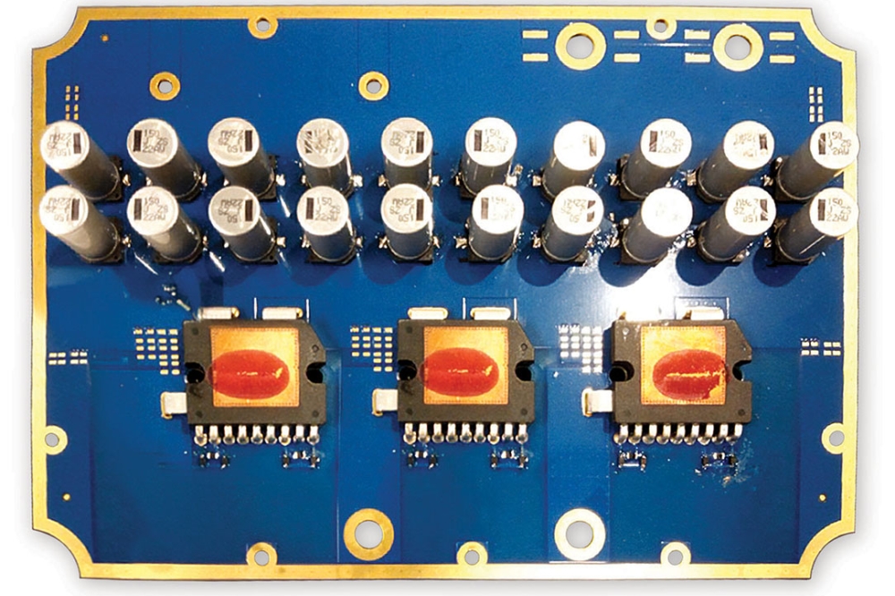
Navitas Semiconductor has launched its new UHV‑TO‑247‑4‑ISO package, purpose‑built for 1200 V to 3300 V GeneSiC SiC MOSFETs.
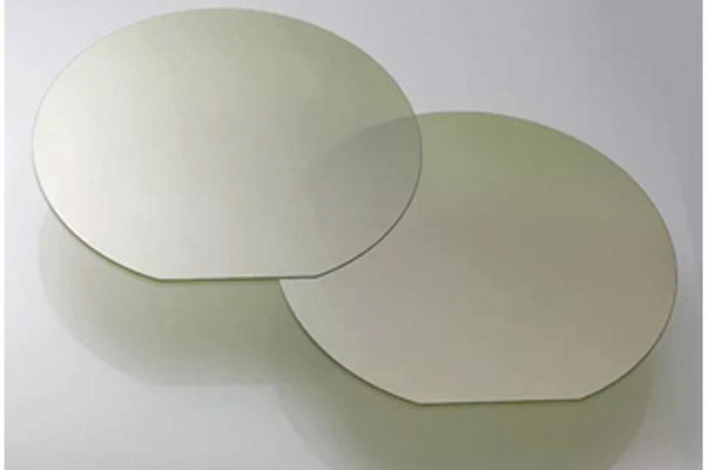
Described as delivering module‑like performance in a compact discrete form factor, the package features over 12 mm pin-to-pin creepage and greater than 6000 V integrated isolation, by integrating an AlN substrate.
It is suited for high-voltage grid-tied power conversion systems (PCS), solid-state transformers (SST), battery energy storage systems (BESS), and renewable energy applications.
When compared with standard non-isolated through-hole packages, the package eliminates the need for external high-voltage isolation, according to the company, and also improves thermal and EMI performance.
A high-voltage isolated, reflow-compatible thermal pad lets the package mount directly to liquid- or air-cooled heat sinks. This leads to up to 150 percent increased power dissipation capability, improving power density, reliability, manufacturability, and overall system cost.
Integrated high-voltage isolation reduces die-to-heatsink stray capacitance compared to external ceramic-based isolators, effectively minimising common-mode noise and radiated EMI. This enables higher switching speeds and delivers improved power density, increased system efficiency, and reduced system-level costs associated with EMI mitigation.
“High-power system design is fundamentally challenged by the need to balance efficient thermal management with robust high-voltage isolation,” said Paul Wheeler, VP and GM of the SiC Business Unit at Navitas. “The UHV-TO-247-4-ISO package overcomes critical thermal and isolation challenges, delivering power module–class performance in a compact discrete form factor. As a highly efficient building block, it empowers system designers to unlock the full potential of GeneSiC TAP SiC MOSFET technology in next-generation applications such as immersion-cooled and liquid-cooled power electronics.”