Two-step anneal aids SiC interfaces
Engineers from the University of Osaka are claiming to have improved the performance and reliability of the SiC-SiO2 interface with a two-step annealing process. Their approach, involving annealing steps in a mixture of argon and hydrogen gas that deliver a hike in channel mobility and improve reliability against bias stress, promises to improve the performance of SiC MOSFETs.
Despite soaring sales, this class of transistor suffers from a high density of interface states that capture free electrons in the channel, leading to an increase in on-resistance, especially for devices with blocking voltages between 600 V and 1200 V.
For many decades, developers and producers of SiC MOSFETs have devoted much effort to trying to improve the quality of the SiC-SiO2 interface, with gains resulting from the incorporation of impurity atoms, such as nitrogen, phosphorous, boron and sodium.
Since the late 1990s, the standard approach for improving the SiC-SiO2 interface is a post-oxidation anneal in nitric oxide. This anneal reduces the density of interface states and increases field-effect mobility, but there is a degradation in reliability – seen, for example, in an instability in the threshold voltage – probably associated with the introduction of nitrogen atoms beside the interface. One significant issue that arises is a degradation in reliability against a negative gate-voltage stress that limits the gate voltage that can be applied to the SiC MOSFET.
Recently, developers of SiC MOSFETs have found that it’s possible to improve the performance and reliability of their devices by minimising the oxidation of SiC during the formation of the gate oxide. This approach supresses carbon-related defects, but as the process relies on interface nitridation, reliability remains a concern.
The novel approach by the researchers from the University of Osaka breaks new ground by improving the reliability and performance of SiC metal-oxide-semiconductor (MOS) devices without resorting to interface nitridation.
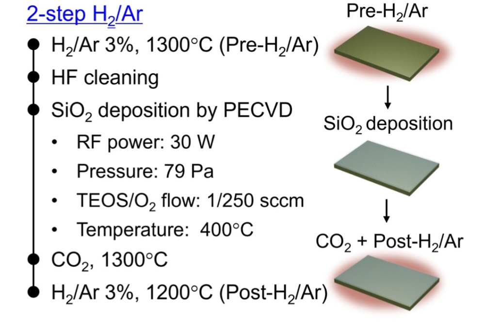
Drawing on an approach widely used in silicon MOS technology, their groundbreaking process is based on dilute hydrogen annealing, and involves annealing before and after gate oxide deposition. The purpose of this two-step anneal is to reduce defects near the surface of SiC, and at the SiC-SiO2 interface. Oxidation of SiC is minimised as much as possible.
The success of this approach has been demonstrated through the fabrication of SiC MOS capacitors and MOSFETs. To produce these devices, the team began by growing an n-type epilayer with a donor density of about 5 x 1015 cm-3 to 2 x 1016 cm-3 for the MOS capacitors, and an n-type epilayer with an acceptor density of about 5 x 1015 cm-3 for the MOSFETs.
Source/drain and body contact regions for the MOSFET were defined by ion implantation through a SiO2capping layer, subsequently removed and replaced with a carbon cap. Argon annealing activated the dopants, prior to removal of the cap by low-temperature oxidation, wet-cleaning of the sample surface and the addition of the gate oxide.
Formation of the gate oxide began by annealing at 1300 °C under a mixture of hydrogen and argon gases, a step designed to remove defects near the SiC surface.
Cleaning of the sample surface in a HF acid solution followed, before plasma-enhanced CVD added a SiO2film. After that the team annealed this structure under CO2 at 1300 °C for 30 minutes, before annealing for another 30 minutes at 1200 °C under a mixture of hydrogen and argon gases.
To evaluate this process, the engineers also produced a portfolio of control samples. One did not have the first annealing step, another had the second anneal in just argon, and samples were also formed by dry oxidation, and oxidation followed by a NO anneal under optimal conditions.
For both capacitors and MOSFETs, oxide thicknesses were 40-50 nm, and electrodes were made of aluminium.
Electrical measurements on the capacitors determined that the team’s two-step process is as effective as NO annealing at reducing the density of interface states.
Note that samples with just a first anneal, or annealing just under argon, have a markedly higher density of interface states.
Secondary ion mass spectrometry revealed that NO annealing led to a concentration of more than 1021 cm-3at the interface of this MOS capacitor, compared with around 1019 cm-3 when using the two-step anneal.
Peak field-effect mobility for the SiC MOSFET produced with the team’s optimised process is 17.2 cm-2V-1 s-1, compared with just 2-3 cm-2 V-1 s-1 for the variant produced by dry oxidation. The engineers attribute this improvement to an increase in free electrons, thanks to a reduction in the density of interface states.
Measurements of the flatband voltage drift are supressed by the two-step anneal in the mixture of hydrogen and argon gas. According to the team, this provides evidence of improved reliability.
Reference
Ref: T. Kobayashi et al. Appl. Phys. Express 18 081002 (2025)