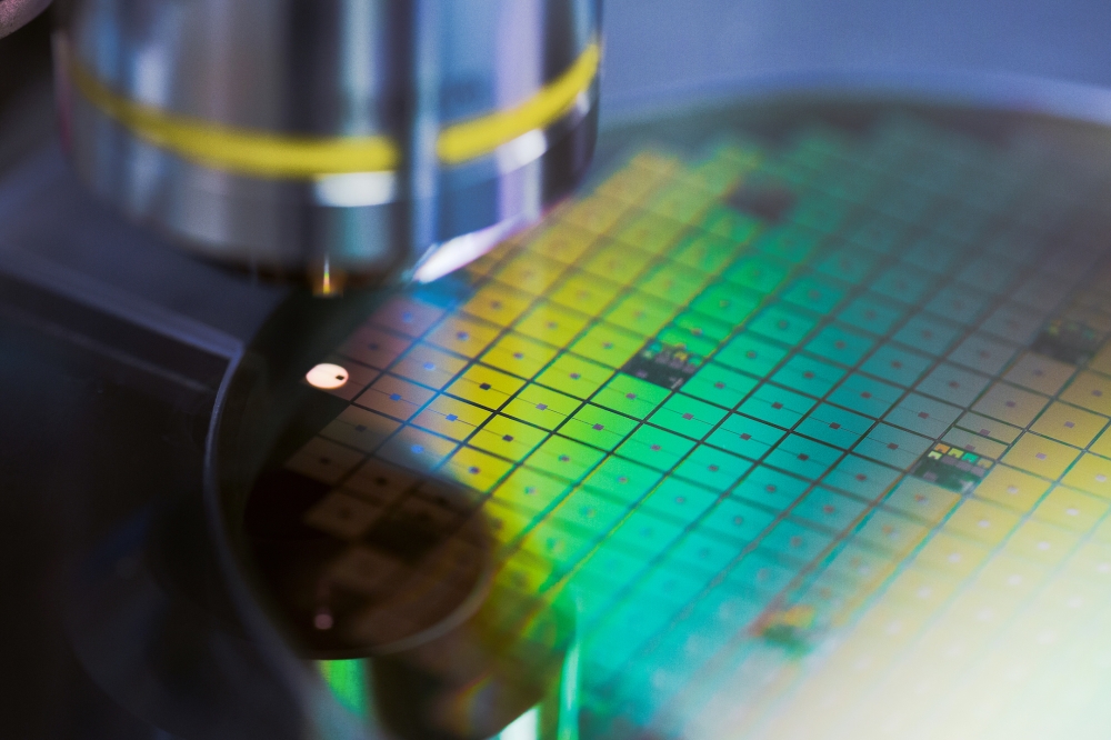
GaN: Reducing the on-resistance of GaN p-n diodes
Engineers from North Carolina State University, Adroit Materials and Poland’s Institute of High-Pressure Physics have reduced the specific on-resistance of vertical p-n GaN diodes formed by magnesium implantation by nine orders of magnitude.
Spokesman for the team, Spyridon Pavlidis, says that this improvement, realised by incorporating magnesium deposition and annealing into the contact stack, has allowed their devices to have a performance on par with those of epitaxial GaN diodes.
The collaboration’s diodes combine excellent rectification ratios with very high current densities and a record-low differential specific on-resistance.
This breakthrough will aid the development of vertical GaN devices that require contacts to magnesium-implanted p-type GaN.
“Ion implantation is a critical part of the semiconductor device processing ‘tool box’, since it enables selective area doping,” says Pavlidis. “This is necessary for manufacturing high-performance transistors and diodes, such as MOSFETs, junction barrier Schottky diodes, and beyond. By controlling where dopants are introduced in the device, we can dictate where current flows and manage electric fields.”
The team’s work helps to address many of the obstacles associated with the realisation of GaN devices that employ magnesium implantation for p-type doping. These challenges include realising: sufficient doping activation and defect mitigation via post-implantation annealing; control of the final dopant profile, due to unwanted diffusion during annealing; prevention of GaN surface decomposition and preservation of electrical properties after annealing; and the formation of high-quality contacts on the implanted structure.
Higher activation energies are produced with ultra-high-pressure annealing, which can also prevent surface decomposition but fails to provide a low-resistance p-type contact.
To address this issue, Pavlidis and co-workers have investigated the impact of physical vapour deposition and annealing of pure magnesium on implanted p-type GaN.
It’s an approach that’s previously been shown to form a low-resistance contact to low-doped p-type GaN, with success attributed to a number of mechanisms. They include: the mutual diffusion of magnesium and gallium, to help create a very heavily doped p-type layer; a reduced barrier height at the metal-semiconductor interface; and the formation of magnesium-intercalated nitride superlattices, introducing ionised acceptors via polarisation.
For the team’s investigation, they produced two vertical diodes – a control, and a magnesium-annealed variant. Device fabrication began by loading n-type GaN substrates into an MOCVD chamber and depositing a 5 µm-thick GaN drift layer with a silicon dopant concentration of around 4 x 1016 cm-3. Magnesium implantation followed, using ion energies of 25 keV and 75 keV and doses of 4.4 x 1013 cm-3 and 2 x 1014cm-3, with a tilt angle of 7 ° to form an initial box of around 100 nm. Samples were than annealed at 1300 °C for 100 minutes undrer 400 MPa in nitrogen gas.
Electron-beam evaporation of nickel and gold added an anode contact to the control, while the magnesium-annealed samples were formed through thermal evaporation of around 60 nm of pure magnesium onto the magnesium-implanted layer using photolithography. Both contacts were subsequently annealed.
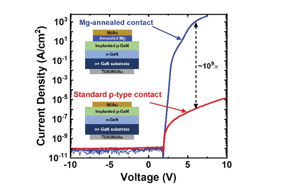
Plots of current-voltage characteristics revealed that the control exhibits expected traits, with an exponential increase in current at an anode bias below 2 V, and a reverse-biased p-type Schottky current-limited regime at higher bias. In sharp contrast, diodes with a magnesium-annealed contact exhibit a repeatable 109improvement in on-current and on-resistance at forward voltages beyond 5 V.
The team attributes these improvements to increased hole conduction through the magnesium-annealed p-type contact. Under a forward bias, the extracted on-resistance is 0.65 mW at an on-current density of around 1 kA cm-2. This is claimed to be the lowest on-resistance for magnesium-implanted p-n diodes, and comparable to vertical GaN-on-GaN epitaxial p-ndiodes. The rectification ratio is more than 1012.
Capacitance-voltage measurements identified a p-type Schottky contact in series with the p-n junction in the control device. With the magnesium-annealed contact this unwanted feature disappears, allowing carriers to be injected into the p-n junction via the anode contact.
Pavlidis and co-workers are now working on improving the contact process and reducing the turn-on voltge for the diodes. “Beyond p-n diodes, we are now applying the combination of implantation and contact technology to more advanced vertical GaN devices.”
Pictured above: Magnesium-annealing improves the performance of p-n diodes, which benefit from the removal of a p-type Schottky contact in series with the p-n junction.
Reference
M. A. Hasan et al. Appl. Phys. Express 18 091002 (2025)